IP-based design has become one of the mainstream methods of FPGA design. This chapter first gives the definition of IP, and then uses the FFT IP core as an example to introduce the application of Xilinx IP core.
5.7.1 IP Core OverviewIP (Intelligent Property) Core is a general term for integrated circuit cores with intellectual property cores. It is a repeatedly verified macro module with specific functions. It can be transplanted to different semiconductor processes regardless of the chip manufacturing process. By the SOC stage, IP core design has become an important task for ASIC circuit design companies and FPGA providers, as well as their strength. For FPGA development software, the richer the IP core provided, the more convenient the user's design, and the higher the market occupancy rate. Currently, IP cores have become the basic unit of system design and are exchanged, transferred and sold as independent design results.
From the way of providing IP cores, they are usually divided into three categories: soft core, hard core and solid core. The hard core cost is the largest in terms of the cost of completing the IP core; in terms of flexibility of use, the soft core has the highest reusability. (This part has already been explained earlier, and I will reiterate it here.)
Soft Core (Soft IP Core)The soft core in the EDA design field refers to the integrated register transfer level (RTL) model; specifically in the FPGA design refers to the hardware language description of the circuit, including logic description, netlist and help documentation. The soft core is only functionally simulated and needs to be integrated and laid out to be used. The advantages are high flexibility and portability, allowing users to self-configure; the disadvantage is that the predictability of the module is low, there is a possibility of error in the subsequent design, and there is a certain design risk. Soft cores are the most widely used form of IP cores.
Solid IP CoreIn the EDA design field, the solid core refers to the netlist with plane planning information; in the FPGA design, it can be regarded as a soft core with layout planning, usually provided in a mixed form of RTL code and corresponding specific process netlist. The RTL description is combined with a specific standard cell library for comprehensive optimization design to form a gate-level netlist, which can then be used by the place-and-route tool. Compared with the soft core, the design flexibility of the solid core is slightly worse, but the reliability is greatly improved. At present, solid core is also one of the mainstream forms of IP core.
Hard IP CoreHard cores refer to proven design layouts in the EDA design landscape; specifically in FPGA design, designs that are fixed in layout and process, verified through front-end and back-end, cannot be modified by designers. There are two reasons why it cannot be modified: first, the system design has strict timing requirements for each module, and it is not allowed to disturb the existing physical layout; secondly, the requirements for protecting intellectual property rights are not allowed to be changed by the designer. The impractical modification of the IP hard core makes it difficult to reuse, so it can only be used in certain applications and has a narrow range of applications.
IP Core Generator is an important design tool in Xilinx FPGA design. It provides a large number of mature and efficient IP Core for users, covering the automotive industry, basic units, communication and network, digital signal processing, FPGA. Features and design, math functions, memory and storage units, standard bus interfaces and other eight categories, from simple basic design modules to complex processors. When used in conjunction with the IP center of the Xilinx website, it can greatly reduce the workload of designers and improve design reliability.
The most important configuration file for Core Generator is suffixed with xco, either an output file or an input file, containing the current project properties and IP Core parameter information.
5.7.2 FFT IP Core Application Example ISE provides FFT/IFFT IP Core, which can perform real-time, complex-signal FFT and IFFT operations. The FFT's IP Core provides three structures, namely:
(1) Pipeline, Streaming I/O structure: allows continuous data processing;
(2) Base 4, Burst I/O structure: Provides data import/export phase and processing phase. This structure has a smaller structure, but the conversion time is longer;
(3) Base 2, Burst I/O structure: uses the least amount of logic resources, the same as Radix-4, providing a two-stage process. The configuration interface has 3 pages, the first page is shown in Figure 5-57, mainly used to configure the implementation structure; the second page configures the data bit width and data processing operations; the third page configures the data cache space.
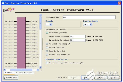
Figure 5-57 User interface of the FFT IP core
In actual hardware operation, the execution speed of the module is a very important parameter, so this paper analyzes the first structure, namely the pipeline Streaming I/O structure, for continuous data processing. When the N-point data of the current frame is performed, the N-point data of the next frame can be loaded, and the N-point data of the previous frame is simultaneously output. This structure is composed of a plurality of base 2 butterfly processing units, each of which has its own storage unit for storing input and intermediate processed data, the structure of which is shown in Figure 5-58.
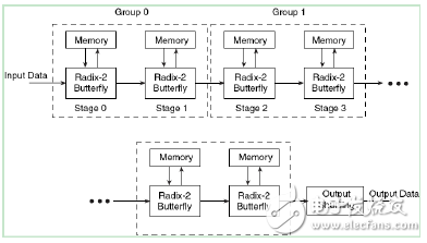
Figure 5-58 Pipeline of the FFT module, Streaming I/O structure
The calculation unit of the FFT has a rich control signal, which is described in detail below.
XN_RE, XN_IM: Input operands, real and imaginary parts, respectively, input in 2's complement. The bit width should be determined when in use.
START : FFT start signal, active high. When this signal goes high, the input data is started, and then the FFT conversion operation and data output are directly performed. A START pulse that allows FFT conversion of a frame. If there is a START pulse per N clocks or if START is always high, then the FFT can be performed continuously. If there is no NFFT_WE, FWD_INV_WE, SCALE_SCH_WE signal before the initial START, the default value of these signals is used after START goes high. Since this IP Core supports non-contiguous data streams, you can start loading data by entering START at any time. When the loading of N data ends, the FFT conversion operation is started.
UNLOAD: For Burst I/O structures, this signal will begin to output the result of the processing. This port is not necessary for pipeline structures and bit-reverse output.
NFFT: This port is only useful for real-time configurable applications.
NFFT_WE : This port is the enable signal for the NFFT port.
FWD_INV: Used to indicate whether the IP Core is an FFT or an IFFT. When it is equal to 1, the IP Core performs an FFT operation, otherwise it performs an IFFT operation. As for which conversion operation is used, it can be changed frame by frame. This port provides great convenience for the use of the FFT.
FWD_INV_WE : As an enable signal for the FWD_INV port.
SCALE_SCH: (1) In the IP Core design, this signal can only work if the intermediate data is reduced during the calculation; (2) The input bit width is equal to 2*ceil(NFFT/2), where NFFT = log2(point size). (3) In the pipeline structure, the butterfly processing unit of each base 2 is regarded as one stage, and the data is reduced once in each stage, and the reduction ratio is represented by two bits of the corresponding stage in the input. (4) The number of two bits per phase can be 3, 2, 1 or 0: they represent the number of bits that the data needs to move.
SCALE_SCH_WE : As an enable signal for SCALE_SCH.
SCLR: Optional port.
Reset : Reset the signal port. When Reset=1, all work is stopped and initialized. But the internal frame buffer retains its contents.
CE: Optional port.
CLK : Input clock.
XK_RE, XK_IM: Output data bus, output in 2's complement. When SCALE_SCH_WE is active, the output bit width is equal to the input; otherwise, the output bit width = input bit width + NFFT+1.
XN_INDEX : The bit width is equal to log2 (point size), the subscript of the input data.
XK_INDEX: The bit width is equal to log2 (point size), and the subscript of the output data.
RFD: Data valid signal, high active, high level when loading data.
BUSY : The indication of the IP Core operating status, which is high when calculating the FFT transition.
DV: Data valid indication signal, which becomes high when there is valid data on the output port.
EDONE: Highly effective. The previous clock goes high when the DONE signal goes high.
DONE : Highly effective. It goes high after the FFT is completed and there is only one clock. After DONE goes high, the IP Core begins to output the calculation results.
BLK_EXP : Available when using Burst I/O structure. If the pipeline is selected, this port is invalid.
OVFLO: Algorithm overflow indication. This signal goes high during data output, such as overflow per frame. This signal is reset at the beginning of each frame.
Example 5.7.1 uses IP Core to instantiate a 16-point FFT module with a bit width of 16 bits.
The Verilog module interface of the multiplier directly generated by IP Core is:
Module fft16(sclr, fwd_inv_we, rfd, start, fwd_inv, dv, scale_sch_we, done, clk, busy, edone, scale_sch, xn_re, xk_im, xn_index, xk_re, xn_im, xk_index);
Input sclr , fwd_inv_we, start, fwd_inv, scale_sch_we, clk;
Input [3 : 0] scale_sch;
Input [15 : 0] xn_re;
Output rfd, dv, done, busy, edone;
Output [15 : 0] xk_im;
Output [3 : 0] xn_index;
Output [15 : 0] xk_re;
Input [15 : 0] xn_im;
Output [3 : 0] xk_index;
......
Endmodule
When in use, you can directly call the mulTIply module, such as
Module fft16(sclr, fwd_inv_we, rfd, start, fwd_inv, dv, scale_sch_we, done, clk, busy,
Edone, scale_sch, xn_re, xk_im, xn_index, xk_re, xn_im, xk_index);
Input sclr , fwd_inv_we, start, fwd_inv, scale_sch_we, clk;
Input [3 : 0] scale_sch;
Input [15 : 0] xn_re;
Output rfd, dv, done, busy, edone;
Output [15 : 0] xk_im;
Output [3 : 0] xn_index;
Output [15 : 0] xk_re;
Input [15 : 0] xn_im;
Output [3 : 0] xk_index;
Fft fft1 ( // call FFT's IPCore
.sclr(sclr), .fwd_inv_we(fwd_inv_we), .rfd(rfd), .start(start), .fwd_inv(fwd_inv),
.dv(dv), .scale_sch_we(scale_sch_we), .done(done), .clk(clk), .busy(busy),
.edone(edone), .scale_sch(scale_sch), .xn_re(xn_re), .xk_im(xk_im),
.xn_index(xn_index), .xk_re(xk_re), .xn_im(xn_im), .xk_index(xk_index));
Endmodule
The functional waveform diagram obtained through simulation test is shown in Figure 5-59:
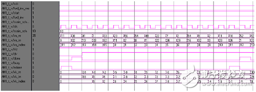
Figure 5-59 IP core simulation waveform of FFT
Distribution Box
Distribution Box,Distribution Boxes TUV,CE Distribution Boxes,Distribution Boxes
Wenzhou Korlen Electric Appliances Co., Ltd. , https://www.zjthermalrelay.com