Overview:
The ECG signal is a bioelectrical signal generated by myocardial contraction and provides information on changes in cardiac physiological function. The measurement electrode is placed in different parts of the body, and the potential difference of different body surfaces is recorded, and the electrocardiogram is obtained. (Electro Cardio Gram, ECG). Because it is easy to detect and has good intuitiveness, it is widely used in clinical medicine. However, the traditional ECG signal acquisition device is large in size and is not convenient for obtaining ECG signals in real time. Therefore, it is important to study portable, low-power ECG signal acquisition systems. Based on the low-power analog front-end ADS1293, this paper combines the MSP430 series low-power single-chip microcomputer to design an ECG signal acquisition system that can be used for ultra-low power consumption and miniaturization.
1 system hardware design ECG signal acquisition system is mainly composed of signal acquisition front-end ADS1293 and MSP430 microcontroller control circuit. The working principle is as follows: the human body ECG signal extracted by the electrode is first sent to the ADS 1293 for proper amplification and then analog-to-digital conversion to become a digital signal. Then, it is sent to the MSP430 MCU through the SPI interface for analysis and processing, and finally sent to the portable display device to display the waveform in real time through the USB interface of the MCU. 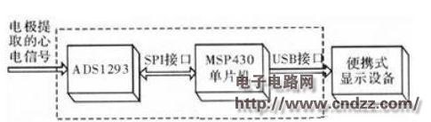
Figure 2 ADS1293 schematic
(1) Signal input interface. There are 6 signal input pins from IN1 to IN6. All input pins contain an electromagnetic interference (EMI) filter to filter out RF noise. The system uses a 5-lead connection, ie the right arm (RA), left arm (LA) and left leg (LL) are connected to the IN1, IN2 and IN3 pins respectively; the common mode detector (CM detect) obtains RA, LA and The average voltage of the LL is used as the input to the right leg drive (RLD) amplifier, and the output of the right leg drive amplifier is returned to the right leg (RL) terminal, which is input from the IN4 pin. The function of the right leg drive circuit is to control the patient's common mode level and increase the AC rejection ratio of the system; the output of the Wilson Network (WCT) is connected to the IN6 pin, together with the V1 (thoracic electrode) connected to the IN5 pin as the CH3 channel. Differential signal input.
(2) Signal processing unit. It is mainly composed of three parts: instrument amplifier (INA), ∑Δ regulator (SDM) and low-pass digital filter (Digital Filter). Its main function is to convert differential analog voltage signals into digital signals. The instrumentation amplifier is an operational amplifier circuit with high input impedance. It has two main functions: 1) Amplifying the differential signal. 2) Provide high input impedance to obtain a larger input signal from the ECG electrode. The output signal of the instrument amplifier is sent to the ∑Δ modulator for analog-to-digital conversion. The ∑Δ modulator is a one-bit coding technique based on oversampling, and the output reflects one bit of the encoded data stream of the input signal amplitude. The low-pass digital filter consists of three programmable 5th-order sin-type filters. The output of the ∑Δ modulator is processed by a low-pass digital filter to obtain an N-bit coded output.
(3) Signal output interface. It mainly includes 4-wire SPI serial interface, DRDYB pin and ALRAM pin. The functions of each pin are as follows: SCLK is the serial clock input pin; SDI is the serial data input pin, a total of 16 bits, of which 1 bit read and write control, 7 bit address and 8 bit data. During the rising edge of the clock, all data is sampled and written to the register on the 16th rising edge of the clock. SDO is a serial data output pin that reads data on the SDO pin on the falling edge of 8 to 15 clocks. CSB is a chip select pin, active low. During low time, the SPI interface starts reading and writing data, and the low level is maintained for 16 clock cycles. DRDYB is the analog to digital conversion end pin, indicating that the internal data of the chip is ready. Readable, active low, usually used as interrupt signal or status inquiry signal of CPU; ALARMB is alarm pin, ADS1293 has a self-diagnosis alarm system for diagnosing abnormal conditions that may occur in ECG applications. Abnormal conditions mainly include electrode dropout, synchronization error, low-power warning and abnormal operation of three channels. When an abnormal situation occurs, it is reported to the error flag and displayed on the ARLAM pin.
1.2 MSP430 MCU control circuit selects TI's ultra-low-power MCU MSP430F5529 as the main controller, which has a wealth of on-chip peripherals, each module runs completely independent, including timer, input/output port, watchdog and UART. It can run independently while the main CPU is in a sleep state. The typical value of current is 290μA/MHz when all modules are active. In standby mode, the typical value of current is only 0.18μA, and the response time from standby to wake-up is 3.5μs. The MSP430F5529 contains two Universal Serial Communication Interface (USCI) modules that support multiple communication modes such as UART, IrDA, I2C, SPI, and USB. In the system, the MSP430F5529 uses the SPI interface to control and transfer data to the ADS1293. The MSP430F5529 operates in master mode and the ADS1293 operates in slave mode. The data is transmitted to the portable display device or computer via the USB interface. Figure 3 shows the interface circuit of the MSP430F5529. 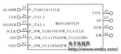
Previous:24V to 5V circuit diagram
Next: Test board
Related Reading
- • [Solution] Application of safety control SCADA system in urban heating monitoring 2016-08-10 14:18
- • [Solution] The tempering furnace acquisition and transmission system based on Dingshengli R-8188 and R-8018 modules 2016-08-10 14:18
- • [Solution] Yokogawa's latest paperless recorder DX2000 in the remote monitoring system of boiler equipment 2016-08-10 14:18
- • [Solution] Multi-parameter telemetry monitoring system based on ZigBee 2016-08-10 14:18
- • [Solution] Introduction of Schneider's complete solution on continuous vertical packaging machine—Schneider Electric (China) Investment Co., Ltd. 2016-08-10 14:18
- • [Solution] Multi-motor power-down synchronous braking of roving frame based on Delta inverter 2016-08-10 14:18
- • [Solution] Schneider's complete solution in the textile printing and dyeing industry - the main chain sub-drive hot air tenter shaping machine control program 2016-08-10 14:18
- • [Solution] Solution of GE Intelligent Platform Products in Power Plant Production Data Monitoring System 2016-08-10 14:18
The Single Most Important Thing You Need To Know About SINGLE SIDED PCB
As a single sided PCB manufacturer, Jinghongyi PCB has been single sided PCB for many years. Production and manufacturing experience, with a very exquisite single sided PCB manufacturing process flow chart.
We can produce single-sided copper PCB, single sided copper clad PCB board, single sided flex PCB.
We know that when you choose single sided PCB manufacturer, product quality is one of the first factors you need to consider. We are not only engaged in PCB manufacturing for many years, but also one of the large-scale PCB manufacturers in China. We can not only produce single sided PCB, but also double-sided PCB, Multilayer PCB , Aluminum PCB and so on.
In addition to product quality, you may also need to consider the single sided PCB price factor. If you choose us as your partner, you can rest assured that we will be able to provide you with not the best price on the premise of guaranteeing product quality, but the price that we both feel is very reasonable. What do you think?
In this article, we will elaborate on the definition, type, cost components, structure, advantages and disadvantages, manufacturing process and raw materials of single sided PCB. Finally, we will introduce the application of single sided PCB and the differences between single sided PCB and Double Sided PCB. And how to choose between single sided PCB and double sided PCB.
What Is Single Sided PCB

Single-sided PCB diagram mainly used Network Printing(Screen Printing), that is, resist on copper surface, After etching, mark the welding resistance, and then finish the hole and the shape of the part by punching.
Fundamentally, single-sided and double-sided printed circuit boards serve the same purpose. Both serve as catalysts for electrical connections between components, however there are some key differences that set them apart from each other. More specifically, they differ in the costs associated with production and development processes, as well as ampacity differences.
With the appearance of electronic transistor, single sided PCB was developed in the early of 1950, which is mainly manufactured in USA. Single-sided PCB was manufactured by copper etching directly at that time. During 1953 to 1955, Japan use imported copper make out paper phenolic aldehyde copper substrate, and apply mainly on radio products. In 1956, single-sided PCB technology was made big progress with the appearance of professional PCB manufacturers from Japan. In the early stage, copper substrate mainly used paper phenolic aldehyde, but because paper phenolic aldehyde with the factors of low electric insulation, bad solder thermal stability, twist issue etc, paper epoxide resin and glass fiber epoxy resin was developed soon after. Currently, paper epoxide resin is widely used in consuming electronic.
Basically, there is no challenge for PCB manufacturer to produce single sided PCB and the technology is quite mature nowadays. The main focus for PCB manufacturer is how to control production cost and save more cost for customers.
Types of Single Layer PCB
- Single Layer Rigid PCB
It is the type of a single layer PCB which is made up a rigid material such as fiber glass. These PCBs are inflexible and prevent the circuit from bending and breaking. Currently these are used in different types of devices such as in calculators and power supplies etc.
- Single Layer Flexible PCB
It is the type of a single layer PCB which is mode out a flexible material instead of a rigid material and for this purpose plastic materials are used. It has so many advantages over single layer rigid pub but it fabrication cost is so much high.
- Single Layer Rigid Flex PCB
It is the type of a single layer PCBs which is used for high frequency circuits normally in giga hertz. These PCBs are made out a Teflon or polyphenylene oxide (PPO) material. During choosing high frequency single layer PCB many aspects are keep in mind such as dielectric loss, thermal expansion and water absorption etc.
- Single Layer High Frequency PCB
It the type of single layer PCBs which is made out by the combination of plastic and fiber glass. Both materials are combined together into single layer. It has so many advantages over single layer rigid and flexible PCB such as it reduces the weight and size of overall PCB.
- Single Layer Aluminum PCB
What Goes Into Determining single sided PCB Costs and price
No matter whether manufacturing a single-sided PCB, double-sided PCB, or multilayer PCB, three main cost categories exist: Primary production costs, dependent costs, and overhead costs.
Often, single layer PCB are used for simple devices and usually cheaper than multilayer PCB.
Multilayer PCB has one or multiple conductor patterns inside the board, this increases the area available for wiring. multilayer PCB, such as 4 Layer PCB , 6 Layer PCB and 8 Layer PCB are usually used for more complicated devices. For example, smart phones use 12 layers due to the various demands of the circuit. As a result, multilayer PCB circuit boards are more expensive.
You can break them down into the following categories:

Layout alters the cost balance. While the number and size of holes remain the same with single-sided PCBs, two different circuit designs on one substrate change the number of holes and add vias.
Because double-sided PCBs welcome complex circuit designs, layout also becomes a dependent factor. As the number of traces increase, costs increase. Smaller surface mount components fastened to the bottom side change the trace spacing. As the space between the traces narrows, costs can jump 5 to 10 percent.
Different layouts may require different hole sizes and the use of laser rather than mechanical drills. Smaller hole sizes and larger hole counts drive the cost higher because of a change in the manufacturing process.
Advantages of Single Sided PCB

- Simple and easy to design and install
- Lower cost, especially for high volume orders
- Easy drilling, soldering, de-soldering and components inserting process
- Lower probability of manufacturing issues,such as short circuiting and producing noise
- Components are installed at only one side, require lower jumper to compensate the circuit
- Popular, common, and easily understood by most PCB manufacturers
- Less time for fault tracing and repairing
Single Layer PCB Disadvantages
Despite their cost advantages and other perks, single-layer boards are not the right choice for every project due to the limitations they have, which include:
- Simplistic Design: The simplicity of single-layer boards' is one of their biggest benefits, but it's also a substantial limitation. For more complex devices that require a higher number of components and connections, a single layer does not provide enough space or power. If wires cross each other, the device won't function properly, so it's critical that the board has enough space to accommodate everything. More complex designs just can't fit on single-sided PCBs.
- Slower Speed and Lower Operating Capacity: The limited number of connections on these boards also affects their power and speed. These less-dense designs are not as robust as those with more circuits and have a lower operating capacity. They might not have enough power for some applications.
- Larger Size and Higher Weight: To add capabilities to a single-sided board, you need to expand its dimensions rather than add another layer, as you could with you a multi-layer PCB. You could use multiple separate boards, but one multi-layer board could likely handle the same requirements. Increasing the size or number of boards in a device also increases your final product's weight.
How to make single sided PCB

Single sided PCB manufacturing Process flow chart
One thin layer of thermally conductive but electrically insulating dielectric is laminated with copper. Soldermask is usually applied on top of the copper.
Cutting - Cleaning - Drilling - Cleaning - PTH - Panel - Plating - Cleaning - Photolithography - Image Transfer - Inspection - Copper/Tin - Plating - Coating - Removing/Etching/Tin - Removing - Inspection - Cleaning - Solder - Mask - Exposure/Develop/Inspection - Prepreg - Screen - HASL - Conformal - Coating - Post - Soldering - Cleaning - Test - Final Inspection - Packing
Single layer PCB Raw Material
- Fr4 Grade Fiberglass Laminates
- Aluminum
- Copper base
- Cem 1
- Cem 3
Construction of Single Sided PCB


The base material, which is also named as substrate, is composed of insulating fiber glass which gives PCB strength and compact look. The nature and type of base material defines if board is going to be Flexible PCB or Rigid PCB.
Above substrate, there lies a copper layer which provides conducting path for various components on the board. The copper thickness is different for different boards depending on your needs and requirements and is defined in ounces per square foot.
On the top of copper foil, there exists a solder mask layer. This layer is mainly used for protection and makes the copper foil insulating which helps in avoiding the conduction in case direct contact happens with some conducting material.
On the top of all layers, there exists a silkscreen layer that is mainly used for adding symbols and characters on the board so a common person can anticipate the clear understanding of the board.
Single-Sided PCB Applications

- Vending machines
- Camera systems
- Surveillance
- Calculators
- Printers
- Solid state drives
- Coffee makers
- LED lighting
- Packaging equipment
- Sensor products
- Power supplies
- Relays
- Radio and stereo equipment
- Timing circuits
What Is Double-Sided PCB

It need circuits on both sides. Via is the holes on boards, coated with metal and it can connect wires on both sides. Because the area of Double-sided PCB is twice as large as the Single-sided PCB, and because the wiring is interleaved, which is better suited for circuits that are more complex.
Someone may feel confused that if one Double-sided PCB, wires on both sides while Electronic parts only one side, is this a Double-sided board or a single onel? The answer is obvious. This kind of board is a Double-sided board, it's just install a component on the Double-sided board.
Differences Between Single sided PCB and Double sided PCB

single sided vs double sided PCB
Single and double sided printed circuit boards share the same material make-up: FR-4, which is a form of fiberglass mixed with epoxy. In modern manufacturing, this is usually layered with copper for conductivity and then coated in solder mask for a professional finish. Sometimes, in a process called silk screening, industrial printers print markings and labels on the board as well.
Single-sided PCBs consist of the FR4 insulating core substrate and a thin layer of copper coating on the bottom or solder-side of the substrate. Through-hole components mount on the top or component-side of the substrate with the leads passing through to the bottom side and soldered to the copper pads and tracks. Surface mount components mount directly to the solder side. The primary difference between the two boards will be in conductor placement.
Double-sided boards rely on the same core substrate but have conductors on both sides of the substrate. Very simply, a double-sided board delivers twice the area for conductors. Complex routing can occur with through-hole components mounted on the top layer and surface mount components mounted on the bottom layer. Plated through holes establish [vias" or the electrical connections between the two sides.
Choose Single Sided PCB or Double Sided PCB?
Which PCB you pick depends on your needs and requirements. Sometimes single sided PCBs are more suitable for project design as compared to double sided PCBs and vice versa.
Before you pick any type of PCB for your project, you must take one thing into consideration that single sided PCB layouts are more difficult to route as compared to double sided PCB, but following are the reasons why you should put an effort for making and picking single sided PCB over other PCBs.
- If you are hobbyist or students, and concerned to make PCB at home, you must know, developing single sided PCBs at home are much easier than developing double sided PCBs at home.
- As you are a manufacturer and very much interested to keep your cost down and producing a single sided PCB a most economical process. In terms of cost, producing single sided PCBs are more economical than producing double sided PCBs.
- Almost all HVAC systems make use of single sided PCBs, because they are more reliable and cost effective and don`t compromise the overall quality of the product.
- Using through hole technology in single sided PCBs still have its drawbacks and limitations because conductive layers, lines and pads stay on single side of PCB but it still is a cheap process to combine all components at one place. Multilayer PCB is also used in many applications where single sided and double sided PCBs fail to fulfill the requirements.
Relationship Resources
Multilayer Metal Core PCB
Single Layer Metal Core PCB
Single Sided Flexible PCB
Single Sided PCB, Single Layer PCB, 1 Layer PCB, making circuit boards
JingHongYi PCB (HK) Co., Limited , https://www.pcbjhy.com