Transformer saturation
Transformer saturation
When starting up under high voltage or low voltage input (including light load, heavy load, capacitive load), output short circuit, dynamic load, high temperature, etc., the current through the transformer (and the switch tube) increases non-linearly. When this happens The peak value of the current cannot be predicted and controlled, which may cause the current over-stress and the resulting over-voltage of the switch tube to be damaged.
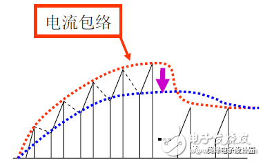
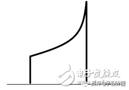 Current waveform when the transformer is saturated
 Susceptible to saturation: - Transformer inductance is too large - too few turns - the saturation current point of the transformer is smaller than the maximum current limit of the IC - no soft start
Solution: - Reduce the current limit of the IC - Strengthen the soft start to make the current envelope through the transformer rise more slowly
2.Vds is too high
Stress requirements for Vds
Under the worst conditions (maximum input voltage, maximum load, highest ambient temperature, power-on or short-circuit test), the maximum value of Vds should not exceed 90% of the rated specification.
Vds reduction method
- Decrease the platform voltage: - Decrease the original primary side turns ratio of the transformer - Decrease the spike voltage:
a. Reduce leakage inductance, transformer leakage inductance is the main reason for generating this spike voltage when the switch is turned on. Reducing the leakage inductance can reduce the spike voltage.
b. Adjust the absorption circuit:
• Use TVS tube • Use slower diodes, which can absorb a certain amount of energy (spikes) • Insert a damping resistor to make the waveform smoother and help reduce EMI
3.IC temperature is too high
Reasons and solutions for excessive IC temperature
- The internal MOSFET loss is too large. The switching loss is too large, and the parasitic capacitance of the transformer is too large, resulting in a large cross-sectional area of ​​the MOSFET turn-on and turn-off current and Vds. The solution is to increase the distance between the transformer windings to reduce the interlayer capacitance. When the winding is wound in multiple layers, a layer of insulating tape (interlayer insulation) is added between the layers.
- A large part of the heat is not good. The heat of the IC depends on the lead to the PCB and the copper foil on it. The area of ​​the copper foil should be increased and more solder should be applied.
- The air temperature around the IC is too high. The IC should be in a place where the air flows smoothly. Keep away from parts with too high parts.
4. No load, light load can not start
Phenomenon: no load, light load can not start, Vcc repeatedly jumps back and forth from the starting voltage and the shutdown voltage.
Causes and solutions: When the load is light and light, the induced voltage of the Vcc winding is too low, and it enters the repeated restart state.
Solution: Increase the number of Vcc winding turns, reduce the Vcc current limiting resistor, and add a dummy load. If you increase the number of Vcc winding turns and reduce the Vcc current limiting resistor, Vcc becomes too high at heavy load. Please refer to the method of stabilizing Vcc.
5. Can not be loaded after starting
Possible causes and solutions:
1. When Vcc is overloaded with heavy load, the voltage induced by Vcc winding is high. When Vcc is too high and reaches the OVP point of IC, it will trigger overvoltage protection of IC, causing no output. If the voltage rises further and exceeds the IC's ability to withstand, the IC will be damaged.
2. Internal current limit is triggered
- When the current limit is too low for heavy loads and capacitive loads, if the current limit is too low, the current flowing through the MOSFET is limited and insufficient, resulting in insufficient output. The solution is to increase the current limiting resistor and increase the current limit.
- The current rise slope is too large. The rising slope is too large, and the peak value of the current will be larger, which easily triggers internal current limiting protection. The solution is to increase the sensitivity without saturating the transformer.
6. Standby input power is large
Possible causes and solutions:
-Vcc is insufficient at no load or light load
In this case, the input power is too high at no load and light load, and the output ripple is too large. The reason why the input power is too high is that when Vcc is insufficient, the IC enters the repeated startup state, and the high voltage is frequently required to charge the Vcc capacitor, resulting in loss of the starting circuit. If there is resistance between the start pin and the high voltage string, the power consumption on the resistor will be large at this time, so the power level of the start resistor should be sufficient.
- The power IC does not enter Burst Mode or has entered Burst Mode, but the Burst frequency is too high
There are too many switching times and the switching loss is too large. Adjust the feedback parameters so that the feedback speed is reduced.
7. Short circuit power is too large
Phenomenon: When the output is short-circuited, the input power is too high and Vds is too high.
Cause: When the output is short-circuited, there are many repeated pulses, and the peak current of the switch tube is very large, causing the input tube power to be too large. The switch tube current stores excessive energy on the leakage inductance, and the Vds is high when the switch tube is turned off.
There are two kinds of output short circuit that may cause the switch to stop working.
- Trigger OCP in such a way that the switching action is stopped immediately. • OCP • Trigger feedback pin stops • Vcc drops to IC turn-off voltage • Vcc rises again to IC startup voltage and restarts
- Trigger internal current limiting When this mode occurs, the duty cycle is limited, and the switching action is stopped by Vcc falling to the lower UVLO limit, and the Vcc falling time is longer, that is, the switching action is maintained for a long time, and the input power will be larger. • Trigger internal current limit, duty cycle limited • Vcc drops to IC turn-off voltage • Switch action stops • Vcc rises again to IC start voltage and restarts
Solution:
- Reduce the number of current pulses, trigger the OCP of the feedback pin when the output is short-circuited, so that the switching action can be stopped quickly and the number of current pulses will be reduced. This means that the voltage at the feedback pin should rise faster when a short circuit occurs. Therefore, the capacitance of the feedback pin should not be too large. - reduce the peak current,
8. No load. Light load output ripple is too large
Possible causes and solutions:
-Vcc is less than Vcc when no load or light load is insufficient. It appears as: oscillating the IC between the start-up voltage (such as 12V) and the turn-off voltage (such as 8V), the IC works in a long interval, providing energy to the short time. The output, then stops working for a longer period of time, so that the energy stored in the capacitor is insufficient to maintain the output stable and the output voltage will drop.
Solution: Ensure that Vcc can be supplied stably under any load conditions.
In Burst Mode, the frequency of intermittent operation is too low. This frequency is too low and the energy of the output capacitor cannot be maintained.
Solution: Increase the frequency of intermittent operation and increase the output capacitance under the condition of meeting standby power requirements.
9. Heavy load, capacitive load can not start
Phenomenon: The light load can be started, and the load can be increased after starting, but it cannot be started under heavy load or large capacitive load.
General design requirements: Whether heavy or capacitive (such as 10000uF), the input voltage is the lowest or lowest, within 20mS, the output voltage must rise to a stable value.
Reasons and solutions (ensure that Vcc is within the normal working range):
The following is an example of a capacitive load C=10000uF. According to the specifications, there must be enough energy to increase the output to a stable output voltage (such as 5V) within 20mS. E=0.5*C*V^2 The larger the capacitance C, the greater the energy that needs to be transmitted from the input to the output within 20mS.
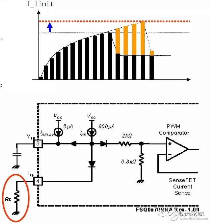
Taking the chip FSQ0170RNA as shown in the figure, for example, the total area S of the shaded portion is the required energy. To increase the area S, the solution is:
1. Increase the peak current limit I_limit to allow a larger inductor current to flow through
The resistance connected to Pin4 is increased, and the shunt from the internal current source Ifb is smaller, so that the voltage at the positive input of the PWM comparator as the current limit reference voltage will rise, allowing more current to pass through the MOSFET/transformer, which can provide more Big energy.
2. At startup, increase the time to transfer energy, that is, extend the rise time of Vfb (before reaching the OCP protection point).
For this FSQ0170RNA chip, the inductor current control is based on Vfb, and the waveform of the Vfb voltage is proportional to the envelope of the inductor current. Controlling the rise time of Vfb controls the rise time of the inductor envelope, ie, the time it takes to transfer energy.
The OCP function of the IC is to detect that Vfb reaches Vsd (such as 6V). So to reduce the Vfb slope, you can extend the rise time of Vfb.
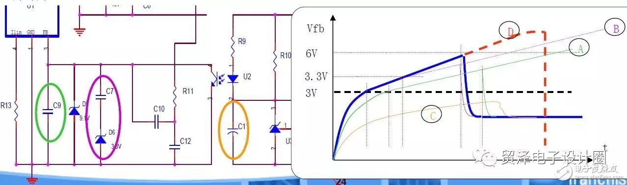
When the output voltage does not reach the normal value, if the feedback pin voltage Vfb has risen to the protection point, the energy transfer time is not enough. When the heavy load and capacitive load start, the output voltage is established slowly, the voltage applied to the optocoupler is low, the current through the optocoupler diode is small, and the photocoupler photocoupler has a high resistance state (which tends to turn off) for a long time. The internal current source of the IC charges the capacitor connected to the feedback pin faster. If Vfb rises to the protection point (such as 6V) during this time, the MOSFET will be turned off. The output cannot reach the normal value and the startup fails.
Solution: When the output voltage reaches the normal value, the feedback pin voltage Vfb is still less than the protection point. Slowly rise Vfb away from the protection point, or extend the time that the feedback pin Vfb rises to the protection point, that is, lower the rising slope of Vfb, so that the output has enough time to rise to the normal value.
A. Increase the feedback capacitance (C9) to lower the rising slope of Vfb, as shown in the figure, from the D line to the A line. However, if the feedback capacitance is too large, it will affect the normal working state, reduce the feedback speed, and make the output ripple larger. So this capacitor can't change too much.
B. Due to the lack of the A method, a capacitor (C7) is connected in series with the Zener diode (D6, 3.3V) in parallel to the feedback pin. This method does not affect normal operation. As shown by the B line, when Vfb <3.3V, the Zener diode will not conduct and shunt. When rising 3.3V, the Zener diode enters the regulated state, and the capacitor C7 starts to charge and shunt, reducing the rising slope of the subsequent Vfb. C. A capacitor (C11) is connected in parallel with the K-A terminal of the 431. When the power is turned on, the C11 voltage is low and is charged by the optocoupler diode and the bias resistor R10 of the 431. In this way, the optocoupler has a large current to pass, so that the impedance of the photocoupler photosensitive tube is low and shunt, and Vfb will rise slowly, as shown by the C line. R10×C11 affects the charging time, which also affects the rise time of the output.
be careful:
1. Increase the feedback pin capacitance (including the Zener string capacitance), which has less effect on solving the problem of large capacitive load. 2. Increase the peak current limit I_limit and also increase the OCP point in steady state. Need to be in the capacitive load, check the transformer to be saturated at the lowest input. 3. If you want to maintain the current limit, you must make R10 × C11 larger, but in the case of large capacitive load (10000uF), it may increase the rise time of 5Vsb more than 20mS. This method needs to check if the dynamic response is too much affected. The bias resistor R10 of 4.431 is too small, and the C11 of 431 parallel is larger. 5. In order to ensure the rise time, the method of increasing the OCP point and increasing the R10×C11 may be used at the same time.
10. No-load, light-load output bounce
Phenomenon: When the output is no load or light load, the input voltage is turned off, and the output (such as 5V) may appear as the voltage debounce waveform as shown in the figure below.
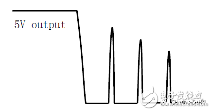
Reason: When the input is turned off, the 5V output will drop, Vcc will also drop, and the IC will stop working. However, when the load is no load or light load, the large PC power supply capacitor voltage cannot be quickly lowered, and the high voltage starter can still be provided. The large current causes the IC to restart, and the 5V re-outputs and rebounds.
Solution: • Insert a large current-limiting resistor into the pin to make the capacitor voltage drop to a high level to provide enough startup current to the IC. • The start is not affected by the large capacitor voltage before starting the connection to the rectifier bridge. When the input voltage is turned off, the startup pin voltage can drop rapidly.

Incremental Encoder,Linear Scale Encoder,Dual Concentric Rotary Encoder,Dc Servo Motor Encoder
Yuheng Optics Co., Ltd.(Changchun) , https://www.yuhengcoder.com