At the end of the keynote speech at Google I/O 2016, Google’s CEO Pippi mentioned a result of their AI and machine learning during this time, a process called Tensor Processing Unit. Device, referred to as TPU. In this month's view, the first generation of TPU processors is outdated.
In the Google I/O 2017 conference held in the early morning of the morning, in addition to promoting Android 8.0, more importantly, Google focused on artificial intelligence, so the second generation of TPU came into being. TPU is a high-performance processor developed by Google independently for AI computing services. Its first generation products have been used in artificial intelligence such as AlphaGo, which is mainly used for computing performance.
Compared with the first generation, the second generation TPU mainly deepens the ability of artificial intelligence in learning and reasoning. As for performance, the new Google TPU can achieve the floating point performance of 180 TFLOPs, which is 15 times higher than that of the traditional GPU. It is 30 times the CPU floating point performance.
In addition, Google has introduced an array of operations called TPU pods, which can contain up to 64 second-generation TPUs, which means that the floating-point performance can reach an astonishing 11.5 PFLOPS.
From the name we can see that the TPU is inspired by the Google open source deep learning framework Tensor Flow, so the current TPU is still only a chip used inside Google.
TPU was bornIn 2011, Google realized they had a problem. They began to seriously consider the use of deep learning networks, which have high computing demands and strained their computing resources. Google did a calculation that would have to double the existing data center if each user used a voice search service based on a deep learning speech recognition model for 3 minutes a day. They need more powerful and efficient processing chips.
What kind of chips do they need? The central processing unit (CPU) is capable of handling various computing tasks very efficiently. But the limitation of the CPU is that it can only handle a relatively small number of tasks at a time. On the other hand, an image processing unit (GPU) is less efficient at performing a single task and has a smaller range of tasks that can be handled. However, the power of GPUs is that they can perform many tasks simultaneously. For example, if you need to multiply 3 floating point numbers, the CPU will be stronger than the GPU; but if you need to do 1 million 3 floating point multiplications, then the GPU will crush the CPU.
The GPU is the ideal deep learning chip because complex deep learning networks require millions of calculations simultaneously. Google uses Nvidia GPUs, but that's not enough, they want faster speeds. They need more efficient chips. A single GPU doesn't consume a lot of energy, but if Google's millions of servers run around the clock, energy consumption can become a serious problem.
Google decided to make more efficient chips.
In May 2016, Google announced the TPU (tensor processing unit) for the first time at the I/O conference, and said that the chip has been used in the Google data center for a year. When Li Shishi battled AlphaGo, the TPU was also applied. In the middle, and Google called the TPU AlphaGo to defeat Li Shishi's "secret weapon."
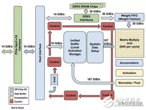
The figure shows the internal structure on the TPU, except for the external DDR3 memory, which is the host interface on the left. Instructions are sent from the host to the queue (no loops). These activation control logic can run the same instruction multiple times depending on the instruction.
The TPU is not a complex piece of hardware, it looks like a signal processing engine for radar applications, not a standard X86-derived architecture. Jouppi said that although it has many matrix multiplication units, its GPU is more sophisticated than the co-processing of floating-point units. In addition, it should be noted that the TPU does not have any stored programs, it can send instructions directly from the host.
The DRAM on the TPU runs in parallel as a unit because more weight is needed to feed the matrix multiply unit (calculated, throughput is 64,000). Jouppi didn't mention how they scaled (systolic) data streams, but he said that using host software accelerators would be a bottleneck.
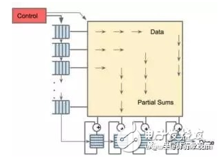
256 & TImes; 256 array scaled data stream engine, realized by nonlinear multiplication after matrix multiplication
As you can see from the second image, the TPU has two memory locations and an external DDR3 DRAM for the parameters in the model. Once the parameters come in, they can be loaded from the top into the matrix multiply unit. At the same time, the activation can be loaded from the left (or output from the "neuron"). Those that enter the matrix unit in a contracted manner to produce matrix multiplications can perform 64,000 accumulations per cycle.
Needless to say, Google may have used some new techniques and techniques to speed up the performance and efficiency of the TPU. For example, use high bandwidth memory or mix 3D memory. However, Google's problem is to maintain the consistency of distributed hardware.
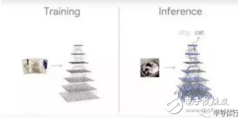
Second generation TPU capable of data reasoningThe first generation of TPU can only be used in the first phase of deep learning, while the new version allows neural networks to make inferences about data. Jeff Dean, head of Google Brain Research, said: "I expect that we will use these TPUs more for artificial intelligence training, making our experimental cycle faster."
“When designing the first generation of TPU products, we have established a relatively complete and excellent R&D team to carry out the design and development of the chips. These R&D personnel are basically involved in the R&D of the second generation TPU. From the perspective of the second generation TPU, compared with the first generation, it is mainly to improve the performance of the single chip from the perspective of the overall system, which is much simpler than designing the first generation TPU chip from scratch. So we can have more energy to think about how to improve the performance of the chip, how to better integrate the chip into the system, and make the chip play a bigger role," Dean said in the speech.
In the future, we will continue to follow Google's progress to learn more about this network architecture. But before that, we should understand the architecture, performance, and working methods of the new generation of TPUs, and understand how TPU performs ultra-high performance computing. At the press conference, Google did not show the chip samples of the new generation of TPU or more detailed technical specifications, but we can still make some speculations about the new generation of TPU from the information we know.
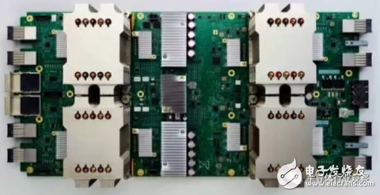
Judging from the TPU picture released this time, the second generation TPU looks a bit like Cray XT or XC development board. From the picture, we can easily find that several connected chips are soldered to the development board while maintaining the connection function between the chips and the chip and the outside. There are four TPU chips on the entire board. As we said before, each individual chip can achieve floating point performance of 180TFLOPs.
There are four external interfaces on the left and right sides of the development board, but two additional interfaces are added on the left side of the board. This form makes the whole board look abrupt. If every TPU chip in the future can be directly connected to the memory, just as AMD's upcoming "Vega" processor can be directly connected to the GPU, this layout is very interesting. The two interfaces on the left side can allow the TPU chip to be directly connected to the memory in the future, or directly connected to the uplink high-speed network for more complicated operations.
All of these are our image-based guesses, unless Google can reveal more chip information. Each TPU chip has two interfaces to connect with external devices. There are two additional interfaces on the left side for external development, which allows developers to design more functions and add more extensions. Whether you connect to a local storage device or a network connection, these features are theoretically feasible. (To achieve these features, Google only needs to establish a relatively loose and feasible memory sharing protocol between these interfaces.)
The diagram below shows a possible form of connection for multiple TPU boards, which Google says can achieve up to 11.5 petaflops of machine learning computing power.
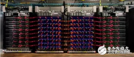
How did this result come about? The connection method above is very similar to an open computer architecture or something else. In the vertical direction, eight TPU boards are superimposed, and in the horizontal direction, four TPU boards are juxtaposed. At present, we can't conclude that each development board is a complete TPU board or a half development board. We can only see that there are six interfaces on one side of the board and two interfaces on the other side.
It is worth noting that there are 4 interfaces in the middle of the board, and 2 interfaces on the left and right sides, and no shell similar to the TPU development board is seen on the left and right sides. A reasonable explanation for this is that the left and right sides are connected to the local memory interface instead of the TPU chip interface.
Even so, we can still see at least 32 TPU second-generation motherboards running, which means that 128 TPU chips are running at the same time. After a rough calculation, the computing power of the entire system is about 11.5 petaflops.
For example, if this computing power can be applied to the commercial field in the future, the 32 current state-of-the-art GPUs used by Google’s large-scale translation work can be reduced to four TPU boards in the future. Can greatly reduce the time required for translation.
It is worth noting that the TPU chip mentioned above is not only suitable for floating-point operations, but also for high-performance computing.
TPU training and learningCompared with the first-generation TPU, in addition to improving the computing power, the second-generation TPU increases the maximum function is the data reasoning ability, but this reasoning model must be trained on the GPU. This training mode makes it necessary for developers such as Google to reduce the speed of the experiment and reshape the training model, which will take longer to get the machine to obtain certain data reasoning ability.
Because of this, iterative engineering is essential for training on relatively simple and single devices and then bringing the results into a more complex environment to achieve higher levels of data reasoning. . In the future, Intel's GPU for artificial intelligence will also adopt this iterative mode. The same is true of NVIDIA's Volta GPU.
The NVIDIA Volta GPU with "tensor core" has ultra-high-speed machine learning and training capabilities, and may reach 120 trillion single-device computing power in the future. This computing power is higher than the Pascal GPU listed last year. About 40%. But the impact of the ultra-high-speed computing power of Google's TPU, even if it's hard to understand in life, the GPU's faster and faster computing power is still impressive, and it's even more us. near.
Dean said that the architecture used by NVIDIA Volta is very interesting, and this architecture makes it possible to accelerate the application through the core matrix. To a certain extent, Google's first-generation TPU has adopted a similar idea. In fact, these technologies are still being used in the machine learning process. “It is always very useful to be able to speed up linear computing,†Dean stressed.
Regardless of the impact of hardware, there are still many places that can attract users. Unlike projects that are always confidential, Google will use TPU technology on the Google Cloud platform in the future. Google's senior researcher Jeff Dean said that they do not want to limit competition through various means, hoping to provide more possibilities and space for TPU, so that they can compete with Volta GPU and Skylake Xeons in the future.
Dean believes that the platform should also provide developers with more opportunities to build and implement their own unique models, rather than limiting the developer's thinking. In the future, Google will provide more than 1,000 TPUs on the cloud platform for research teams interested in open research projects and continuous machine learning.
Dean said that now in Google, when training and learning machines, the GPU and CPU will be used at the same time, which is also true on the same device, which can better ensure the balance. But for the new generation of TPU chips, the power of training and learning is not yet accurately estimated, but it is worth noting that the function is definitely lower than the Volta GPU. Because the system is functionally capable of high performance computing and 64-bit high performance computing, this makes workload calculations extremely complex. NVIDIA's GPU will encounter similar problems during its use. In the future, if we want to solve this problem better, we need to continue to work hard with engineers.
At this point, Dean also admits: "Unlike the first-generation TPU chip's integer calculation, the second-generation chip can perform floating-point operations. So in the process of learning and training the chip, only a fixed model is needed. There is no need to change the algorithm. Engineers can use the same floating-point operation, which greatly reduces the workload."
In addition to NVIDIA and Intel, Google has brought its customized hardware products to market, which is not a good thing for enterprises. Because TPU is still a fairly marginal technology for the market. When the second-generation TPU products are applied to the Google Cloud platform, Google will push training to a large number of users, which will better promote the development of this technology.
For those who don't commercialize the chip for Google, the above content can give an answer. With the continuous development of artificial intelligence and neural learning technology, TPU will be able to make a big impact on Google Cloud and become a force to promote technological progress.
What does TPU mean for Google?A software engine developed by Google for deep neural networks. According to Google, according to the growth rate of Moore's Law, the computing power of the current TPU is equivalent to the calculation level that can be achieved in the next seven years. Each watt can provide a higher order of instruction for machine learning, which means it can use fewer crystals. Do each operation, that is, do more in one second. And Google has deepened its binding with the Deep Learning system platform TensorFlow to get better support and a stronger ecosystem, including more than 100 projects that require machine learning technology, including search, driverless cars, and smart voice. .
Is TPU the future of deep learning?Chip deployment in deep learning calculations is not a zero-sum game. Real-world deep learning networks require the system's GPU to communicate with other GPUs or ASICs such as the Google TPU. The GPU is the ideal work environment with the flexibility you need for deep learning. However, ASICs are ideal when they are completely dedicated to a software library or platform.
Google's TPU clearly meets this requirement. The superior performance of the TPU makes it possible for TensorFlow and TPU to be upgraded together. Although Google officials have repeatedly stated that they will not sell TPUs. However, third parties who use Google Cloud Services as a machine learning solution can benefit from the superior performance of the TPU.
The smart chip market has changed, and the emergence of Google TPU has made the trend of chips that accelerate the specific domain of neural network/deep learning more obvious. High-end AI applications require powerful chips to support them. The lack of software and hardware in China's smart ecology will not develop. China's processor academics and engineering are constantly improving. We look forward to China Core's early sunrise and now on the world stage to compete with international counterparts.
LANA Vape Stick 1500 Puffs is so convenient, portable, and small volume, you just need to take them out of your pocket and take a puff,
feel the cloud of smoke, and the fragrance of fruit surrounding you. It's so great.
We are China leading manufacturer and supplier of Disposable Vapes puff bars, lana vape stick 1500 puffs kit,lana vape stick 1500 puffs plus,
lana vape stick 1500 puffs rechargeable, and e-cigarette kit, and we specialize in disposable vapes, e-cigarette vape pens, e-cigarette kits, etc.
lana vape stick 1500 puffs kit,lana vape stick 1500 puffs plus,lana vape stick 1500 puffs rechargeable,lana vape stick 1500 puffs vape pen,lana vape stick 1500 puffs box
Ningbo Autrends International Trade Co.,Ltd. , https://www.supervapebar.com