
In conventional switching power supplies, magnetic components are often used for filtering, energy storage and transmission. The higher the operating frequency of the switching device, the smaller the size of the magnetic component , and the easier it is to achieve miniaturization, weight reduction, and cost reduction of the power supply device. However, an increase in the switching frequency will correspondingly increase the switching loss of the switching device, so soft switching technology has emerged.
To achieve an ideal soft-switch, the best case is to turn the switch off and on (ZVS, ZCS) when both voltage and current are zero, so that the loss is truly zero. To achieve this goal, resonant techniques must be employed.
Second, LLC series resonant circuit

The principle of the circuit, in series or parallel LC resonant circuit may be configured such that when the power source is a DC power supply circuit to obtain a current change according to the sine law. Since the current or voltage changes according to the sinusoidal law, there is a zero crossing. If the switching device is turned on or off at this time, the loss generated is zero. The LLC resonant half bridge circuit currently used is analyzed below. The basic circuit is shown below:
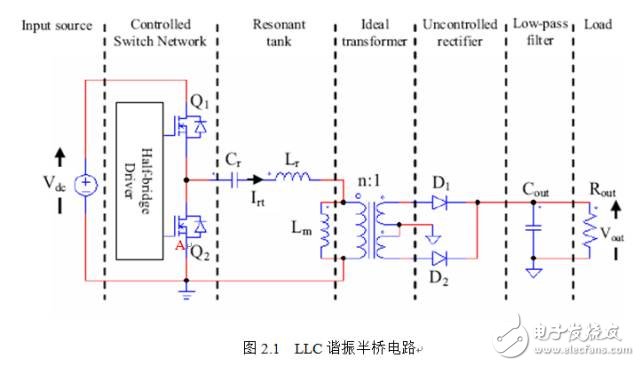
Among them, Cr, Lr, Lm constitute a resonant cavity (Resonant tank), so-called LLC, Cr acts as a DC-blocking capacitor, while balancing the transformer flux to prevent saturation.
2.1 LLC circuit characteristics
(1) Frequency conversion control
(2) Fixed duty cycle 50%
(3) There is a dead time between the switch tube and the turn-on, so the Mosfet can be turned on (ZVS), and the secondary side can be turned off at zero point, so the diode recovery loss is small.
(4) High efficiency, can reach 92%+
(5) Smaller output chopping, better EMI
2.2 Square wave Fourier expansion
For the half-bridge control circuit of Figure 2.1, Q1, Q2 are alternately turned on in one cycle, that is, the duty cycle is 50%. So VA is a square wave, the amplitude is equal to Vin, and its Fourier series is expanded to

Its fundamental component is

Where fsw is the switching frequency and V o.FHA (t) is the fundamental component of the square wave voltage input to the cavity.
Correspondingly, the resonant cavity output voltage (ie the ideal transformer output) is also a square wave.

Its fundamental component is

Where Ψ is the phase shift of the output voltage relative to the input voltage, which is virtually zero.
2.3 FHA circuit model
By making the equivalent transformation of the nonlinear circuit of the circuit shown in Figure 2.1, the following figure can be obtained:
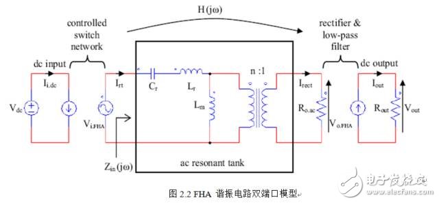
FHA (First harmonic approximation): First harmonic approximation principle. The principle assumes that the transmission of energy is only related to the fundamental component of the voltage and current Fourier expressions in the resonant tank. Therefore, if the influence of the switching frequency is ignored, the cavity is excited by the sinusoidal input current Irt, and its expression is:

Where is the phase shift of the input current relative to the input voltage.
Correspondingly, the resonant cavity output current irect is

Since Vo.FHA(t) is in phase with irect(t) , the output impedance of the resonant circuit is

Where Rout is the load impedance, and the impedance is converted to the reflection resistance Rac of the primary side of the transformer.

Therefore, the input impedance of the cavity Zin(s) is

Transformer gain transfer function H(S) is

The voltage gain M(fsw) is

2.4 Voltage gain M (fn, λ, Q) analysis
Replace the variables in the voltage gain M(fsw) expression to get the functions of the three parameters fn, λ, and Q. The new expression is

The parameters in the formula are defined as follows:
Resonant frequency

Characteristic impedance

Quality factor

Lr and Lm inductance value ratio

Normalized frequency

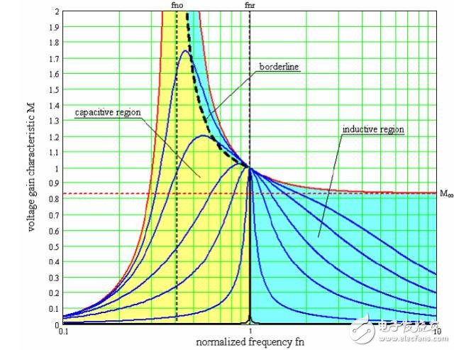
When making λ=0.2, the cluster of M(fn, λ, Q) curves is as follows:
(horizontal axis is fn and vertical axis is M)
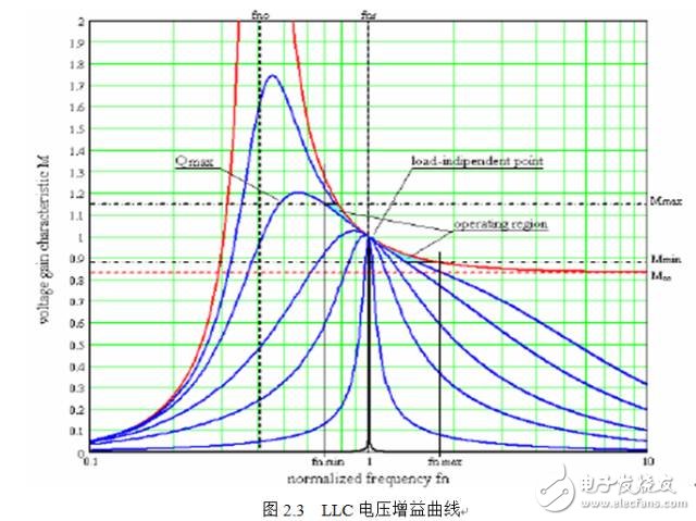
The red curve is the voltage gain curve MOL at no load (Q=0). As fn tends to infinity, MOL gradually tends to M∞.

As can be seen from the figure, for different Q-value curves, the Load-independent point (fr, unity gain) is passed, and the tangent slope of all the curves at this point is -2λ. Fortunately, the load-independent point appears in the inductive region of the voltage gain characteristic curve, where the cavity current lags behind the input voltage square wave (this is a necessary condition for ZVS).
By changing the square wave voltage frequency of the input resonant tank, the output voltage of the converter can be stabilized: since the working area is the inductive part of the voltage gain characteristic, when the output power is reduced or the input voltage is increased, the output voltage is stabilized by increasing the operating frequency. . With this in mind, if the converter operating point is close to the load-independent point, then the stability of the output voltage will be inversely proportional to the wide load variation, and accordingly the switching frequency will vary over a small range.
Obviously, the wider the input voltage range, the wider the operating frequency range will be, and therefore, it is difficult to optimize the circuit design. This is also a common shortcoming in all current resonant topologies.
In general, high-power applications generally have a primary PFC circuit. For wide voltage inputs (85Vac ~ 264Vac), it will boost to 400V after PFC, and the range of variation is not large (10% ~ 15%). Therefore, for the LLC circuit with PFC on the front end, the fluctuation of the LLC input voltage is small, so the above problem is not very serious.
The operating voltage variation range is: the minimum operating voltage is determined by the PFC pre-regulator's hold-up capability during the mains dips; the maximum operating voltage is determined by the threshold of the OVP line. Therefore, when the input voltage is at a normal value, the resonant converter can optimize the design at the load-independent point, and the minimum input voltage during the mains dips is given to the boosting capability of the resonant cavity itself. (eg the operating point is below the resonance point)
In addition, it is also possible to obtain a resonant frequency fo at no load (secondary Diode non-conducting)

2.4.1 Selection of Mmin and fmax
When the input voltage Vdc is maximum and the output load is minimum, the voltage minimum gain Mmin must be greater than M∞

The maximum normalized frequency is

2.4.1 Selection of Mmax and fmin
When the input voltage Vdc is minimum and the output load is maximum, the voltage minimum gain Mmax

The minimum normalized frequency is

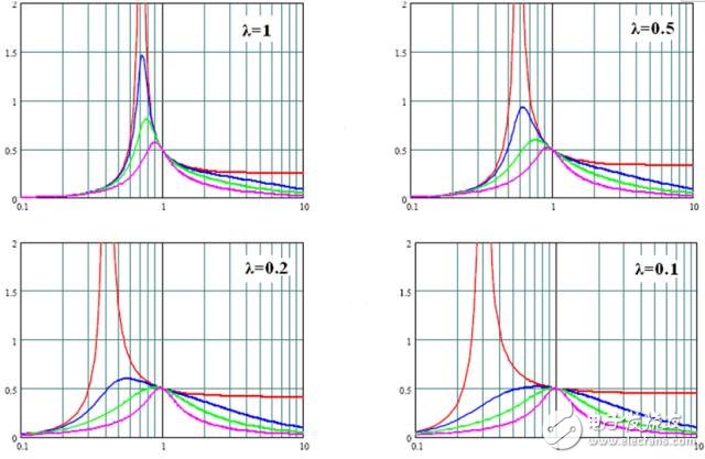
Regarding the analysis of λ, the corresponding change in λ is:
(1) The gain curve on the M-fn plane shrinks toward the resonance frequency fnr, which means that the no-load resonance frequency fno increases;
(2) The asymptote line M∞ of the no-load gain characteristic is gradually reduced;
(3) The maximum gain of each gain curve increases.
2.4 Normalized impedance Zn(fn, λ, Q) analysis

When making λ=0.2, the Zn(fn, λ, Q) curve cluster is as follows:
(horizontal axis is fn and vertical axis is Zn)
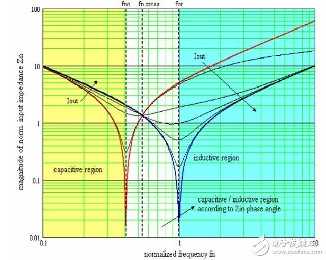
Among them, the red and blue curves are normalized impedance curves for no-load and short-circuit, respectively. All Zn are asymptotic with two normalized resonant frequencies fno and fnr, and curves with different Q values ​​intersect at a point. , the normalized frequency of the point fn.cross:

When the operating frequency is greater than the crossover frequency fcross, the input impedance decreases as the output current increases. When the operating frequency is less than the crossover frequency, the input impedance increases as the output current increases. The output impedance is always reduced.
According to fn, the whole picture can be divided into three sections.
Fn
Fn>fnr inductive workspace
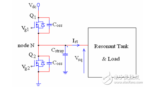
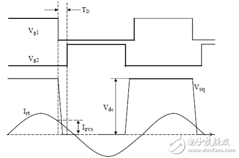
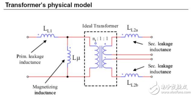
Fno Off-topic, evaluate the efficiency of the converter by impedance characteristics η input power Output Power So efficiency η Wherein Y in.LOSS admittance input impedance (admittance), the input impedance is equal to the inverse (reciprocal) Assuming that the imaginary part of Zn is zero, that is, Zin is zero phase (the characteristic impedance Zo is the true value and does not affect the phase), the critical frequency fz of the LLC resonant converter operating in the inductive and capacitive regions can be solved and normalized. Processing gets: Where fnz is only related to the fixed λ-Q, at which point the input cavity impedance is only the real part (only useful work is absorbed from the power supply). At the same time, you can get the maximum quality factor Maximum quality factor Qmax: When less than Qmax, the resonator impedance is inductive for the same fn-λ, therefore, the maximum voltage gain Mmax Bring Qz(fn, λ) into M(fn, λ, Q) to obtain an expression such as Mz (fn, λ) Therefore, the part between fnr and fno can draw Mz (fn, λ) to determine the boundary line of the inductive and capacitive boundaries, as shown in the figure below. As can be seen from the figure, for a single Q-value curve, the maximum Gain point always falls in the capacitive area 3.1 Overview It is assumed that the inductive region is only a negative condition of the half-bridge MOSFET ZVS, not a sufficient condition, because the parallel capacitance of the midpoint of the half bridge (ignored in the FHA analysis) requires charging during the conversion process ( Charged) and depleted. In order to understand the working situation of ZVS, refer to the following figure There are two capacitors, which are the equivalent drain-source capacitance (output capacitance) Coss of the POWER MOSFET and the cavity impedance stray capacitance Cstray, so the total capacitance Czvs at the node N is The conversion process is as follows 3.2 ZVS sufficient conditions In order to achieve ZVS, there is a dead time TD between the turn-on of the two MOSFETs. Since the operation is in the inductive region, the input current lags behind the input voltage. When the half cycle ends, the current Irt of the cavity is still flowing. This current can consume the charge stored on the Czvs, so that the voltage of the node N drops to zero. So zero voltage is turned on when the other switch is turned on. At the end of the half cycle, the current in the resonant current cavity must be guaranteed to consume the charge of Czvs in TD time. This is the sufficient condition for ZVS, and the critical current Izvs is This current is equal to the peak value of the reactive current flowing through the cavity (90 degrees out of phase), which determines the reactive power of the circuit. Active current input current Iact So input current Irt Phase Φ of the cavity current hysteresis voltage (input impedance phase of the operating point) So we can get the phase judgment of the sufficient condition of the half-bridge POWER MOSFET ZVS in the whole working interval. 3.3 Ensure the realization of ZVS by selecting Qmax Qzvs1 under full load Finding tan Φ is not convenient for solving the quality factor (full load, minimum input voltage, maximum gain, minimum operating frequency), so we calculate Qmax (maximum output power, minimum input voltage), and the input impedance is zero phase (from above) As can be seen from the description of Qmax, Qmax is obtained under the condition that the Zn imaginary part is zero, that is, the phase Φ is equal to 0, and the zero phase cannot satisfy the sufficient condition of ZVS, that is, the Irt at the end of the half cycle does not Greater than the critical value Izvs), so choose the difference (5%-10%) to ensure that the phase Φ is not zero: The results obtained from the above formula are to verify whether the conditions of tan are met. If they are not satisfied, they need to be redesigned. Qzvs2 under no-load conditions Of course, the sufficient conditions of ZVS need to meet the situation of no-load and maximum input voltage, so that the maximum quality factor of ZVS at full load increases the constraint Qzvs2 . When no load, Q=0, so and Known by ZVS Simplify the above formula to obtain the quality factor at no load and maximum input voltage Therefore, in order to ensure that the cavity can be ZVS throughout the working range, the maximum quality factor Qmax must be less than min (Qzvs1, Qzvs2) Referring to the voltage gain characteristics in the above figure, it is assumed that the cavity is designed to operate in the inductive region with the maximum output power Pout.max, correspondingly, Q = Qmax, and assume that the gain of the output voltage relative to the input voltage is greater than 1, as shown in the figure M = Mx As the output power gradually increases from zero to the maximum value, the corresponding gain for different loads will gradually enter the black curve (Q = Qmax) from the red curve (Q = 0). The control loop will keep M always equal to Mx, so the quiescent point will move along the horizontal line of M=Mx. Correspondingly, the abscissa of the intersection of the horizontal line M=Mx and the Q value curve is under different load conditions. The working frequency. If the load increases beyond the maximum specified value Q=Qmax, the operating point of the last converter must enter the capacitive region. At this time, the MOSFET hard switch will occur, and if there is no corrective action, it may cause equipment failure. In fact, if Q is sufficiently large relative to Qmax, the intersection with M=Mx will appear in the left half plane of the boundary line Mz, that is, the capacitive region; if the tangent of the Q value curve exceeds M=Mx, the working point will not Will move along M=Mx. This means that the converter will not guarantee the stability of the output voltage, although the operating frequency will decrease (feedback reversal), but the output voltage will still drop. Limiting the minimum operating frequency (M=Mx and Q=Qmax at the intersection abscissa) does not prevent the converter from entering the capacitive working area. In fact, when the operating frequency reaches the minimum value, if the load continues to increase, it will cause the working point to move along the vertical line by f=fmin and finally through the dividing line. Limiting the minimum operating frequency is only effective if the minimum operating frequency is greater than 1 after normalization. Therefore, considering the overload and short circuit of the output, the converter's work frequency must be greater than the resonant frequency fr to reduce the power throughout. It is worth noting that if the converter specifies that the peak output power (the output voltage must be maintained) is much larger than the maximum continuous output power for a limited time, the cavity must be designed with peak output power to ensure that it does not enter capacitive operation. Interval. Of course, the thermal design can only consider the maximum continuous output power. In any case, no matter how the converter is specified, a short circuit or a general overload condition (beyond the maximum cavity specification) requires additional means of processing, such as current limiting circuits. The LLC resonant half bridge is ideal for magnetic integration, for example, to concentrate inductors and transformers into a single magnetic device. This can be easily seen from the physical model of the transformer , and it is clear that a topology similar to the inductance portion of the LLC circuit can be seen. However, the ideal transformer has leakage inductance on the secondary side, which was ignored in the previous discussion. In order to consider the effect of the secondary side leakage inductance into the FHA analysis, we learn a special transformer model and a simplistic assumption. It is well known that there are many alternative electrical equivalent models for a given transformer due to the many choices of the ideal transformer ratio in the model. For a suitable "equivalent" circle ratio n (obviously different from the physical circle ratio nt = N1: N2), all components related to the leakage flux can be equivalent to the primary side. This equivalent model is called APR (All-Primary-Referred), that is, all parameters are equivalent to the primary side, and the model satisfies the FHA analysis. The APR model can be obtained by selecting n: k : transformer coupling coefficient L1: primary side winding inductance value L2: single-sided secondary winding inductance value note: (1) Lr still maintains the meaning in the physical model: the primary side inductance value measured when short-circuiting the secondary winding (2) The primary side inductance L1 cannot be changed. The difference between the two models (physical model and APR model) is only in the way of segmentation, so the difference between L1 and Lr is Lm. Finally, if these parameters are clarified by the equivalent APR model, the above analysis can be directly applied to transformers in the real world. Vice versa, the design flow based on FHA analysis will provide parameters for the APR model; therefore, steps must be added to determine those parameters in the physical model. Especially when calculating the nt (physical model), since Lr and Lm are related to the real world, Lr+Lm= L L1+Lμ=L1 In the physical model, the problem cannot be solved mathematically: because there are 5 unknowns LL1, Lμ, nt, LL2a, LL2b ; and there are only 3 parameters in the APR model: Lr, Lm, n. The assumption that overcomes this problem is based on magnetic circuit symmetry: it is assumed that the leakage fluxes of the primary side and secondary side windings are just equal. This assumes that you can get: 3.1 Design Specifications Input voltage range: Vdc.Min-Vdc.max Normal input voltage: Vdc.nom Output voltage: Vout Resonant frequency: fr Maximum operating frequency: fmax Starting frequency: fstart 3.2 Additional Information Shunt capacitance of node N: Czvs Dead time: TD 3.3 General Design Guidelines Criterion 1: Converter design works at nominal input voltage Criterion 2: The converter must be able to automatically adjust when the input voltage is maximum and zero load Guideline 3: The converter must be working in the ZVS area all the time 3.4 10 design steps 1) It is known from criterion 1 that, under normal input voltage, the gain of the resonant frequency point is equal to 1, and the transformer (APR) ratio is calculated: 2) Calculate the maximum and minimum gains by taking the extreme values ​​of the input voltage range 3) Calculate the maximum normalized operating frequency by definition 4) Calculate the equivalent load impedance reflected to the primary side of the transformer 5) Calculate the maximum input voltage, maximum operating frequency, and zero-load condition, the inductance ratio λ 6) Calculate the minimum input voltage, the maximum Q value in the ZVS region at full load (select 90% to 95%) 7) Calculate the maximum input voltage, the maximum Q value of the ZVS region when no load is applied 8) Select the entire working range (no load to full load) to allow the maximum Q value, ie Qzvs 9) Calculate the minimum input voltage, the minimum operating frequency at full load 10) Calculate the characteristic impedance of the cavity and all component values ​​(Lr, Lm, Cr) 








Barium titanate lead-free piezoelectric ceramics are important basic materials for the development of modern science and technology, which was widely used in the manufacture of ultrasonic transducers, underwater acoustic transducers, electroacoustic transducers, ceramic filters, ceramic transformers, ceramic frequency discriminators, high voltage generators, infrared detectors, surface acoustic wave devices, electro-optic devices, ignition and detonation devices, and piezoelectric gyroscope and so on.
Application: military, ocean, fishery, scientific research, mine detection, daily life and other fields.
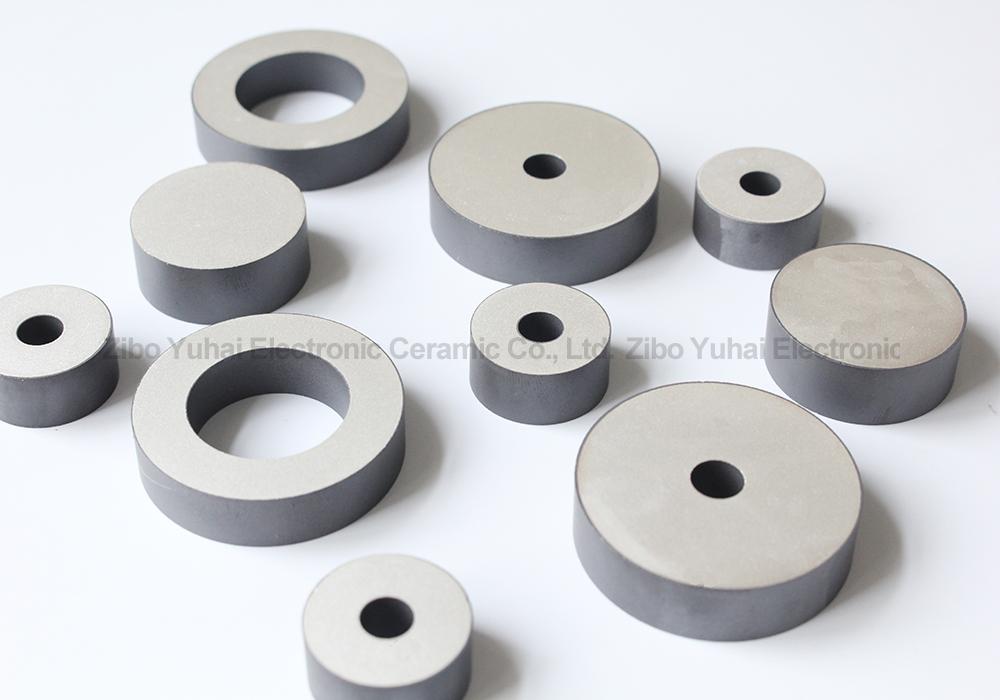
Piezoelectric Ring,Lead Free Piezoelectric Ring,Piezo Electric Ring,Lead Free Piezo Rings
Zibo Yuhai Electronic Ceramic Co., Ltd. , https://www.yhpiezo.com