With the rapid development of computer and digital image processing technology, video surveillance technology is widely used. Traditional video surveillance systems use a single camera to monitor a fixed scene. Not only does the video have a limited field of view, but it cannot monitor different orientations of the same object. Here, a multi-channel video surveillance system is proposed to monitor different scenarios by stably and reliably switching control of different video channels. The system not only makes up for the limited shortage of traditional surveillance video, but also improves the utilization of monitoring resources and reduces the monitoring cost.
1 The hardware structure of the system adopts the hardware structure scheme of DSP+FPGA, and uses DSP and FPGA to control the video channel required by the MAX4312 strobe, so as to achieve the purpose of switching between multiple video channels. The system structure block diagram is shown in Figure 1.
This article refers to the address: http://
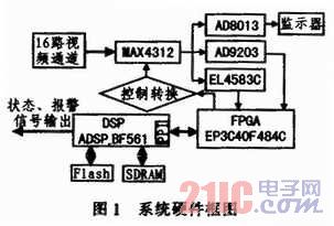
1.1 Control device selection According to actual needs, DSP uses Blackfin series high-performance processor ADSP_BF561 (hereinafter referred to as BF561) introduced by Analog Devices as the algorithm processing and control core. BF561 processor contains 2 independent BF533 cores, each The core contains two multiply/accumulate (MAC), two 40-bit ALUs, four video ALUs, and one 40-bit shifter. The Blackfin processor features an improved Harvard architecture and a hierarchical memory structure. L1 memory typically runs at full speed with little or no delay. L2 is another level of memory that is distributed on-chip or off-chip and consumes multiple processor cycles for its access. At L1 level, the instruction memory only stores instructions, two data memories store data, and a dedicated temporary data memory stores stack and local variable information. At the L2 level, a unified storage space is used to store instructions and data. Here L2 level memory is used.
The FPGA preprocesses the video signal with Altera's EP3C40F48C, which has up to 24,624 logic cells with an advanced external memory interface that allows external single data rate (SDR) SDRAM, double data rate (DDR) SDRAM and DDR FCRAM devices are integrated into complex system designs without degrading data access performance, with 129 compatible LVDS channels, data rates up to 640 Mb/8 per channel, and 4 programmable phase-locked loops and 8 global clocks line. In addition, the power consumption of the EP3C40F484C is low, and the total power consumption during global operation is about 300 mW.
1.2 Flash design According to the needs of system design, Flash uses CMOS type M29W640D, and its space is 18 Mx16 bit. In this system, the external data lines are D1 to D15, and the address lines are A2 to A22. Note that when connecting, because Flash is 16 bit wide, the address of the hardware needs to be misaligned, that is, A2 of DSP corresponds to A1 of Flash, A3 of DSP corresponds to A2 of Flash, and so on. In software programming, any operation on Flash, such as erasing and writing, must first write a certain number of fixed control command words to a specific address, that is, a check-in instruction, so as to ensure that when power-on and power-off, it will not Memory misoperation.
1.3 SDRAM Design The external data memory used in this system is the large-capacity SDRAM MT48LC16M16, which has a capacity of 4 Bankx8 Mx16 bit. According to the actual requirements of the system design, SDRAM stores real-time image data, reference data, and program code while the system is running. Since the access speed of Flash is relatively slow, in the system initialization, the reference data and program code stored in the system should be moved to a faster memory in advance, so that the DSP is not restricted by the memory reading time. Its high speed performance.
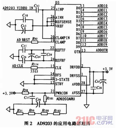
1.4 Video acquisition module design Because the switching time of the video channel is very short, this requires the switching control module to have a very accurate judgment of the video signal, so as to send the switching command in time, so it is necessary to select a high-speed converter. In addition, since the system's power supply is 5 V, it is necessary to select a low-power device. Therefore, the AD9203 is selected as a digital quantizing device for analog signals.
The AD9203 is a single-channel, low-voltage, high-speed A/D converter from Analog Devices that has a sampling rate of 40 Ms/s. Its accuracy is stable and reliable, and it always maintains 10-bit accuracy in the full sampling bandwidth. At 40 Ms/s sampling rate, ENOB (effective number of bits) still reaches 9.55 bits, and differential nonlinearity is ±0. .25 LSB, signal-to-noise ratio and distortion are maintained at around 59 dB. The AD9203's flexible operating voltage allows for variations from 2.7 to 3.6 V, making it ideal for high-speed operation of portable devices at low voltages. With a supply of 3 V, the power consumption is only 74 mW at 40 Ms/s full speed; at 5 Ms/s, the power consumption is reduced to 17 mW, and in standby mode, the power consumption is only 0.65 mW. For the peak-to-peak value of the input signal, it is usually set to 1 Vp-p or 2 Vp-p. In addition, the AD9203 allows an external voltage reference, which can flexibly set the peak-to-peak value of the input signal between 1 and 2 V depending on the design requirements. Figure 2 is a schematic diagram of the circuit application of the AD9203.
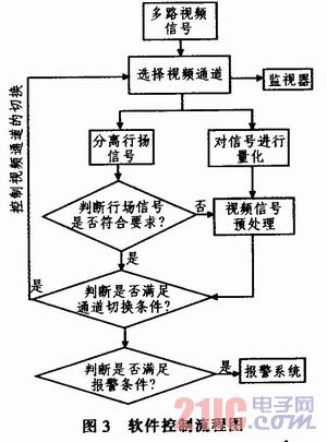
2 Control module design The workflow of the whole system is to install multiple cameras for image monitoring at different monitoring points. The multi-channel image and video signals pass through the MAX4312, and one of the video signals is input at each moment. The video signal is processed by the AD8013AR to output a digital image signal from the image monitor, and the corresponding line (VIDEO_Hs) and field (VIDEO_Vs) signals are output from the line separation chip EL4583C, and the image back shoulder signal (AD_BRST) and video quantization are output from the AD9203. signal. The line (VIDEO_Hs), field (VIDEO_Vs) signals are then sent to the DSP, and the back-shoulder signal (AD_BRST) and the video quantized signal are sent to the FPGA. The FPGA uses these signals to preprocess the image, and then sends the processed image to the DSP through the PPI port for algorithm processing. Finally, the DSP sends a video channel switching command to complete the switching between different channels, and sends the final processing result to the alarm and status indicating device to implement the monitoring alarm function. The software control process is shown in Figure 3.
2.1 FPGA module power rudder buy
The FPGA control section is used to preprocess the video signal and wait for the DSP to send a handover command. The basic idea is: When a certain video signal passes through the AD9203, the output video quantized signal is sent to the FPGA for preprocessing, and then sent to the DSP for algorithm processing, while the FPGA waits for the DSP to switch the video channel according to the field signal.
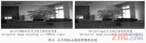
During the experiment, it was found that the DSP search for the image is triggered by the rising edge (or falling edge) of the row signal, so the row signal needs to have a stable rising edge (or falling edge). Since the signal may generate jitter during the separation and transmission, the rising edge (or falling edge) of the signal is unstable, which affects the judgment of the DSP on the video signal. If this unstable line signal (VIDEO_Hs) is still used as the mark of the DSP search image, the image received by it will be misaligned in the adjacent two lines, and the image drift phenomenon seen by the naked eye. The image (a) in Fig. 4 is an image received with the VIDEO_Hs signal as a flag. This requires the FPGA to de-jitter the line (VIDEO_Hs) signal, but the signal received by the FPGA is only the line signal separated by the EL4583, and the specific position of the rising edge (or falling edge) of the signal cannot be resolved. Therefore, the FPGA generates 1 row flag signal (H_flag) as needed to replace the unstable row signal (VIDEO_Hs), and then sends the row flag signal (H_flag) and the field signal (VIDEO_Vs) to the DSP to make accurate video signals. judgment. The image of (b) in Fig. 4 is an image received with the H_flag signal as a flag.
2.2 PPI port settings
Data communication between the FPGA and the DSP is implemented through the PPI port. The PPI (Parallel External Interface) is a half-duplex form with a bidirectional port for up to 16-bit data input and output. The PPI has 5 memories to control its operation. The PPI control register (PPI_CONTROL) sets the operating mode of the PPI port, the polarity of the control signal, and the bandwidth of the port. In this design, set PPI_CONTROL to 0x00EC, set the working mode of PPI to ITU_656 mode, set the width of port to 8 bits, and only the mode of receiving data. Since each PPI_CLK_initiated event (ie, an input or output operation) on the DMA bus processes 16 as an entity, that is, if the transmitted data is not 16 bits, the high bit of the data is padded to 16 as data. In this case, a more effective method is to pack the data, that is, combine the 8-bit data transmitted by the two FPGAs into one 16-bit data, and then transmit the data, thereby effectively utilizing the resources and improving the transmission efficiency.
2.3 DSP control function implementation
To implement the DSP control function, first set the PF pin of the DSP to determine the interrupt signal on the PF pin. The communication between the FPGA and DSP interrupt signals is defined by PF6 and PF7, and then the DMA (Direct Memory Access) is set. When the video signal is processed, the odd-even field signals are processed separately, that is, only processed at a certain time. An odd field or an even field of the signal to increase the processing speed of the signal. This requires storing the parity fields of the video signal separately. When the DMA is set, the parity field signal data is stored under different addresses.
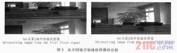
When the DSP receives the signal sent by the FPGA through the PF pin, it begins to implement its control function. The specific control switching process is as follows: when the DSP receives the first VIDEO_Vs signal transmitted by the PPI port, the DSP starts the video through the field counter (VsCount). The signal is counted, and then the value of VsCount is read. When the count of VsCount reaches the switching requirement, the DSP will send a switching command to the FPGA, that is, write a value under an address, and let the FPGA complete the video through the DSP_A and DSP_D read commands. Channel switching. Since the field signals of the two channels may be out of synchronization before and after the video channel switching, the image is searched in the second field after the channel switching. Figure 5 shows the DSP receiving from the first field and the second field respectively. The result of the image.
3 System test results The experiment switches 24 video signals, and sets the switching time of each video signal to 6 fields, that is, the video channel is switched once every 6 fields. The settling time between different video channels will not exceed one field, that is, the two channels can be stabilized within one field after switching. The experimental results show that the system can realize the switching between multiple video channels stably and reliably. It can add multiple cameras to monitor different scenes in real time on a set of monitoring equipment, which not only effectively solves the single monitoring target of traditional monitoring system. The shortcomings, but also improve the monitoring efficiency and reduce the monitoring cost.
4 Conclusion First, the hardware architecture and chip performance of the whole system are briefly introduced. The workflow of the whole system is described. Then, the control and gating of multiple video channels by DSP and FPGA are emphasized. The entire FPGA design program is written in the Verilog hardware description language on the Quartus II platform. The DSP program is successfully compiled in VisualDSP++, both of which have been verified by multiple debugging. The system design has been successfully applied to the multi-scene monitoring alarm system to accurately and reliably switch between different video channels.
Anderson Plug Flush Mount,Anderson Plug And Socket,Smh Connector,Anderson Plug,Anderson Connector
Dongguan Andu Electronic Co., Ltd. , https://www.idofuse.com