The semiconductor industry is currently facing a dramatic change in integrated circuit (IC) manufacturing methods that are designed to continuously improve the performance and density of ICs and may impact design methods. Wafer foundries are currently preparing to enhance the 14nm and 16nm processes using 3D transistor structures based on the finFET concept, as they offer higher performance than 20nm planar transistors.
By increasing the current-carrying channel, it can be surrounded by the gated three, so that the gating exhibits stronger static control. This overcomes the short channel effects that lead to excessive leakage currents and other problems that arise with nano-planar transistors fabricated using a large number of silicon wafers.

  Figure 1 better illustrates leakage current control over the frequency range
A further advantage of multi-level gating is that the drive current in the unit range is more than the drive current in the unit range of the planar device - compared to the planar device, the fin (Fin) is used with the same equivalent gate length. The height of the structure creates a channel with a larger effective volume. This means better effective performance.
By enhancing the FinFET performance, a higher number of frequencies than bulk silicon technology can be achieved with a given power budget. The reduction in power consumption stems from two aspects: reduced demand for wide high-drive standard cells; and the ability to operate at lower supply voltages given the amount of leakage current. However, only a change in design technology can fully achieve power reduction performance.
Standard cell-based processes are still a key factor in achieving high productivity IC implementation. Over the past few decades, unit extraction has cemented the foundation of the integrated drive design process, providing the foundation for highly automated digital circuit implementation, enabling small-scale teams to design millions of gate-level circuits. Transistor structure changes and associated layout-dependent effects are about to break through the clear interfaces before the physical, cell, and logic layers of the design flow, which necessitates designers to consider low-level features when laying out circuits. However, by enhancing cell-level intelligence, the productivity advantages of standard cell extraction can be maintained and the power, performance, and area (PPA) advantages achieved by finFET-based processes can still be obtained.
Accompanying the finFET is a fundamental change in the circuit structure due to its shape change (Figure 2). The fin structure of a given process has a fixed width and spacing. Compared to planar processes (which can increase the overall drive strength by any amount of transistor width to improve the performance of large sectors or high capacitance buses), the effective width of finFETs can only be achieved by adding more fins to the transistors. Change it. Fin (Fin) structure quantization not only increases the complexity of analog and custom circuit design, but also has a subtle and important impact on digital circuit implementation.
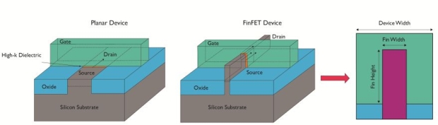
Figure 2 FinFET vs planar transistor
In summary, finFET-based processes will benefit from the narrowest possible fin spacing (Fin), as this will provide better density, flexibility and performance. The process used to create the fin structure relies on a chemical auto-alignment technique that reduces the line spacing of the finest layers (M1 and M2) that are spaced apart from the metal by 25%. These metal layers are currently drawn using two masks that are irrelevant but combined into a synthetic exposure, rather than using a self-aligning process. The minimum spacing of these metal layers is determined by the stacking error, so a self-aligned fin (Fin) structure forming step can achieve higher spacing. When designing a standard cell for most digital logic (which will be used in finFET-based ICs), you need to consider the Fin structure's mismatch with the M2 spacing (typically, the Fin structure is parallel to the M2 spacing). ).
For finFET-based processes, there are only a few effective "gear ratios" between the Fin structure and the wide spacing of the metal conductors that produce a viable standard cell library, so it needs to be designed so that each cell has a A fixed number of routing paths. Even so, some combinations can cause the metal mesh to be inflexible, making it difficult to carry enough current for the cells on the critical path. Nano-processes are increasingly being affected by effects such as electromigration, which reduce the life cycle of ICs by thinning the metal wires through strong currents until they disappear.
For maximum metal wiring density, the design rule for dual masks applies not only to the wide spacing of metal wires, but also to their width. The result of this is that a wider metal wire cannot always be drawn to carry the high current required to provide a unit with high driving force. The ratio of the number of fin structures to the number of metal conductors allows for a more flexible use of the metal interconnect process in power supply routing. They support the use of a wider, more flexible power rail when needed, while the number of routing paths in the cell provides a higher logic routing density to carry power. To take advantage of the above structure, you need to understand the standard cell architecture based on the traditional place-and-route tools you usually know. The place-and-route tool is designed to use standard units as a set of I/O and power pins at predetermined locations. Black box.
Tools that can use their understanding of the internal standard cell architecture and remap cells based on logical requirements can additionally provide the flexibility needed to take advantage of the new architecture described above without having to completely reorganize the IC implementation process. The same understanding can help other design processes adopt the latest design changes to produce an Engineering Change Order (ECO).
Since design rules are more restrictive than ever, implementing ECO becomes more difficult because even a small change can cause problems with the mask color of the dual mode layer. The process of integrating tools that understand the local standard cell environment can be designed deeper to implement ECO as transparently as possible.
An in-depth understanding of the internal architecture of standard cells will help solve other problems arising from migration to finFET-based nanofabrication. As designers try to take advantage of the higher performance of 3D transistors and speed up the clock, they will face even more severe variability challenges. Although finFETs exhibit less variability in some key metrics than planar transistors, variability is still a major obstacle to timing termination, and the boundaries between standard cells and routing layers exist in a variety of ways.
Traditionally, such variability will be integrated into the guard band that limits clock speed, hindering the performance gains achieved by the finFET structure. Better analysis and correction techniques can largely restore such performance loss, speeding up clock speeds and making products more competitive in the marketplace.
The dual-mode technology used in 14nm and 16nm finFET-based processes has been shown to result in huge path delay differences. For example, a small transition in aligning one of the reticle for the imaging interconnect mode can increase the coupling capacitance between the gate electrode and the cable, thereby increasing the path delay. Since the transition of the entire reticle will become uniform, the delays associated with the reticle mode will be correlated - more advanced analysis tools that understand each standard cell behavior and internal connectivity will also be considered. By considering the above correlation and taking corrective measures, the concern about the difference in coupling capacitance can be eliminated and the target clock speed can be increased.
Interconnect parasitics, especially the high resistance of metal wires in finFET-based processes, will also hinder the performance of the clock tree. The clock tree uses a large number of long-distance connections to keep the timing of the ICs consistent. Traditional technologies such as buffer insertion will increase energy consumption. By using the knowledge of basic standard cells, you can perform smarter clock tree optimizations, provide low-deviation timing signals, and avoid spending power budgets.
Reducing device geometry also increases the likelihood of single event disturbances due to ionizing radiation, resulting in incorrect results and system crashes. Analysis of cell structures in a circuit environment (possibly replacing them with enhanced versions) can reduce the likelihood of misbehaving in the presence of alpha particles.
This move with a finFET-based process will result in a number of process-level changes and will have an impact on digital design. If left unresolved, it will result in poor IC performance. While these physical effects can threaten extremely stable and standard cell-based processes, the introduction of tools that address SoC designs at the cell level will help maintain process stability and fully realize the benefits of finFET-based processes.
LVLP series Linear Power Supplies are DC Power Supplies that achieve AC/DC conversion through power frequency transformers and transistor loop control. Compared with switching DC power supplies, linear mode power supplies have higher stability, higher accuracy, and lower output ripple. And the most important, because of the use of the power frequency AC/DC conversion principle, the linear power supply does not have high-frequency radiation interference, and is especially suitable for use in places with restrictions on EMC and EMI.
The LVLP series linear AC - DC power supplies have a wide range of output specifications, the output power ranges from 1KW to 400KW, and the output voltage can reach up to 800VDC, and accept customization.


The whole series DC linear power supply adopts industrial-grade metal chassis, pure copper AC/DC varnished transformer, high-reliability multi-transistor filter loop, ensuring the power supplies can run for a long time at full load with high stability, high accuracy, and ultra-low ripple electronic characteristics, equipped with a complete protection circuit, which can better ensure the reliability of the linear power supply itself and the safety of the customer's load.
The output voltage and current can be adjusted by the 10-turn potentiometer with scale and lock on the front, equipped with 4 1/2-digit high-resolution LED meters for output value reading, and RS communication interface can also be added for remote control and monitoring of linear power supplies.
This series of linear power supplies are mainly used for aging and testing of components such as capacitors, relays, and resistors, and can also be used for experimental testing of electronic components such as thermistors and motors. At present, many well-known capacitor manufacturers, resistor factories and other electronic component production units and scientific colleges and universities and other research and development units use this series of power supplies, and they have all been highly praised.
Linear DC Power Supplies, Linear AC - DC Power Supplies, DC Linear Power Supplies, AC - DC Linear Power Supplies, Linear AC DC Supplies
Yangzhou IdealTek Electronics Co., Ltd. , https://www.idealtekpower.com