Based on the download control mode of the FPGA basic data stream, the genetic algorithm is used to program and configure the FPGA through the MCU to control the data stream to realize its own reconstruction, so that the system has the characteristics of self-adaptation, self-organization and self-repair.
This paper implements the hardware evolution process based on genetic algorithm. The population is randomly generated by Mcu, and the selected genes are cross-mutated to generate offspring, and then the appropriate gene is tested to find the best reconstruction plan. Choose the best solution to apply to the hardware to achieve self-healing and self-adaptive.
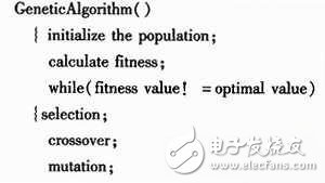
1 Software algorithmGenetic algorithm (GeneTIc Algorithm, GA) is an adaptive global optimization search algorithm proposed and gradually developed by Professor John Holland of the University of Michigan in the 1970s. He simulates the reproduction, crossover, and gene mutation phenomena that occur in natural selection and natural genetic processes. He retains a set of candidate solutions in each iteration, and selects the better individuals from the group solutions according to a certain index. Individuals combine to generate a new generation of candidate solution groups until a certain convergence index is met, and finally the optimal or approximate solution of the problem is obtained.
The basic genetic algorithm consists of 4 parts: (1) coding (generating the initial population). (2) Calculation of fitness function. (3) Genetic operators (selection, crossover, mutation). (4) Operating parameters.
1.1 Selection
The genetic algorithm must first generate an initial population, usually called a chromosome. Chromosomes are composed of genes, such as 11001, each binary number is a genetic variable, and then the qualified chromosomes are detected by the fitness function, and the qualified chromosomes are selected for the next crossover and mutation to obtain new individuals.
The fitness in the genetic algorithm refers to the adaptability of an individual to the environment, and also the ability of the individual to reproduce offspring. The fitness function of the genetic algorithm is also called the evaluation function. It is an index used to judge the degree of the individual in the group. It is evaluated according to the objective function of the problem sought.
Here, the mode of the fitness selection function adopts a feedback mode to evaluate the generated individuals through simulation. If the requirements are met, the evaluation results are stored in the storage module, and then all the function results are weighted in a roulette manner to determine the ratio of the fitness of each gene to the weighted sum, that is, a decimal between (0, 1), Select a value greater than a value such as 0.8 to be qualified. After evaluating the fitness of all individuals in the group, select individuals with fitness greater than 0.8 to store, and then wait for new individuals generated by the cross-mutation module.
1.2 Cross mutation
The cross mutation module obtains two individuals from the selection module, and compares the random number generated by the random number module with the cross probability to determine whether to perform the cross operation. The crossover operator randomly exchanges two genes in the population according to the crossover rate, which can generate new gene combinations, and hope to combine beneficial genes together.
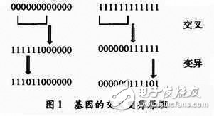
If you find two parent genes, you need to intersect, find the intersection of the genes, and cross the gene variable of each gene to form a new gene variable. The mutation is to find the gene mutation point for each gene and try to find the appropriate one through gene mutation. The scheme is shown in Figure 1.
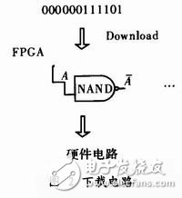
1.3 Gene download
The excellent gene obtained is the required solution. Download this solution directly, and finally achieve controllable, reconfigurable and adaptive. as shown in picture 2.
The basic genetic algorithm is to abstract the object as a string arranged by a specific symbol in a certain order through a certain coding mechanism, just like the chromosome is a string arranged by genes. Here, binary coding is used, and the 5 bit binary characters string. The procedure is as follows:
At present, mainstream FPGAs all use a look-up table structure based on the SRAM process, and some military products and aerospace-grade FPGAs use a look-up table structure of Flash or fuse and anti-fuse technology. The method of changing the content of the look-up table by programming files to achieve the repeated configuration of FPGA.
Look-up table (Look-Up-Table) is abbreviated as LUT. Currently, 4-input LUTs are mostly used in FPGA, so each LUT can be regarded as a RAM with 4-bit address line. In this way, each input of a signal to perform a logical operation is equivalent to entering an address to look up the table, find out the content corresponding to the address, and then output.
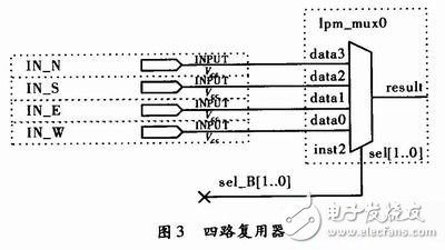
2.1 Multiplexer (MulTIplexer)
Based on the principle of this 4-input LUT structure, a 4-input multiplexer is used. In the process of multi-channel data transmission, any one of them can be selected as required, also called a multi-channel selector or a multi-channel switch. In this paper, the 5-bit data stream generated by the controller controls the selection of four input ports through a shift register, as shown in Figure 3.
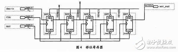
2.2 Shift Register (Shift Register)
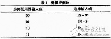
In digital circuits, registers are usually used to store binary data or codes, as shown in Figure 4. The data generated by the Mux selection bit is output by the controller after being buffered, and SelA [1, 0] and SelB [1, O] act on the two multiplexers respectively. The control bits of the output control multiplexer in the shift register are shown in Table 1.
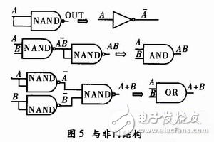
2.3 NAND gate
NAND gates are the basic gates that make up various circuits. Different gates can be built with NAND gates as needed. As shown in Figure 5, different NAND gate structures can be used to realize other functions such as AND gates or gates to achieve dynamic Refactoring.
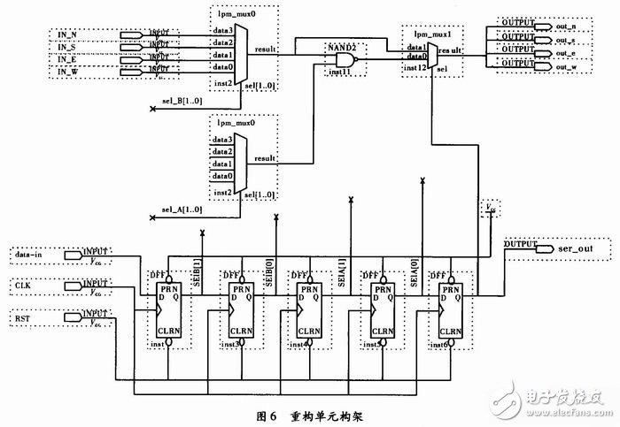
3 Unit structure of reconfigurable systemAccording to the structure principle of the 4-input LUT, this circuit selects two 4-input MUX to select the input port of the NAND gate, and then uses a 2-input MUX to select the data output, and the three MUX selection bits use SelB [ 1, 0], SelA [1, 0], Sel-out control, the shift register serves as a buffer of 5-bit serial binary numbers, as shown in Figure 6. It can be seen that the NAND gate can form a variety of digital circuits through the selection of 4 inputs from east, west, south, and north. This unit structure can continue to be expanded to 2 & TImes; 2 or more units to realize complex digital circuits. The simple structure of AND gate and OR gate formed by the unit structure is demonstrated here, which further illustrates the realizability of reconfiguration.
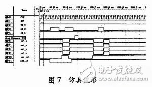
When the generated data stream passes through the buffer to reconstruct the circuit, you can see the functions implemented by the new familiar circuit, as shown in Figure 7. By observing the relationship between the input and output terminals, the best solution of the required circuit can be obtained by testing, which can be downloaded to the hardware and complete the required tasks.
The hardware structure is based on the communication between the microcontroller and the FPGA. Mcu selects MSP430, communicates with FPGA through RS232, and the PC downloads the program to the central chip through the JTAG interface. In the peripheral equipment, select 2 8-bit LEDs, 4-bit input buttons, 1 12864 LCD display, reserve 32-bit expansion interface. As shown in Figure 8, the FPGA chose Ahera's EP1C16Q240C8.
5 SummaryThe implementation of circuit reconfigurable technology has become a new hotspot in the research of computing systems. The hardware is gradually softwareized. It is configured by a microprocessor combined with multiple FPGAs to achieve dynamic local reconfiguration. It has strong versatility and Adaptive, suitable for modular design. Based on the 5-bit data stream, this article implements part of FPGA dynamic reconfiguration, which can generate the required hardware structure in real time. Dynamic reconfiguration can make full use of reconfigurable hardware, especially reconfigurable computing. The technology has developed greatly in theory. One of the future development directions of FPGA is to support SOPC hardware that can be dynamically configured.
Vertical Mount Power D-SUB Connectors
ANTENK launches series vertical board mount Power-D & Combo-D D-SUB connectors machined contacts.
The ANTENK Power-D & Combo-D mixed contact d-sub connectors straight are designed for rugged / robust applications where both power & signal are required from a single connection. Featuring [Solid-Pin" machined contacts, these connectors offer high reliability performance for the most challenging design applications.
vertical board mount Power-D & Combo-D D-SUB connectors machined contacts applications
The ANTENK vertical mount combo d-sub, mixed contact connector product range is ideal for a multitude of both IP rated and non-rated industry applications. This diverse combo d-sub standard product offering includes up to 13 contact configurations (seen below) engineered for both power & coaxial connector environments such as satellite & weather stations, GPS receivers, transceivers and radio technology applications. Contact us directly for any custom or semi-custom combo d-sub connector project not listed in our standard product offering above.
Features of Vertical Mount D-SUB Connector Machined Contacts
Available in 12 industry standard sizes / positions.
Contact Antenk for other sizes / contact configurations.
Available in 10/20/30/40 amp power contacts, 5 amp signal
Allows signal, high current & high voltage in one connector.
Contacts are pre-loaded into the insulator.
Material of Vertical Mount D-SUB Connector Machined Contacts
Shell: Steel, Nickel plated
Insulator: Glass-Filled Thermoplastic, U.L. 94V-O, Black
Signal Contacts: Machined Copper Alloy, Full Gold Flash
Power Contacts: Machined Copper Alloy, Full Gold Flash
Male High Density Power D Mixed Contact Connectors, Female High Density Power D Mixed Contact Connectors, Male Standard Vertical Mount Power D-SUB Connector, Female Standard Vertical Mount Power D-SUB Connector
ShenZhen Antenk Electronics Co,Ltd , https://www.antenkelec.com