Main control board hardware system structure
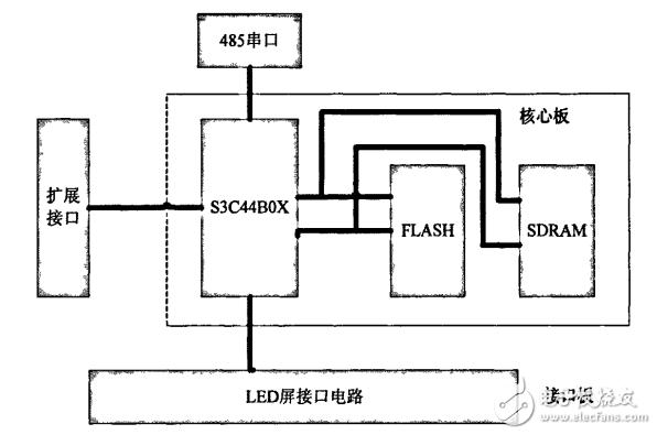
Figure 3-3 Hardware structure block diagram
The main control board of a large LED display system should be able to perform the following functions:
(1) The bitmap code and the display mode that the PC side sends to request display are received and stored.
(2) Sort the original dot matrix codes according to the display mode to meet the DMA transmission data requirements.
(3) Mapping the sorted dot matrix code to the column data latch of the corresponding display position of the LED display screen and controlling the line drive cyclic scan display.
According to the system requirements and future expansion requirements, the system structure block diagram is shown in Figure 3.3. The system design adopts the separate design of the core board and the interface board, which enhances the flexibility and scalability of the system application. The inside of the dotted line in the figure is the core board, and the outside of the dotted line is the interface board to the LED display. The core board completes tasks (1), (2), and (3). The interface board performs logic functions such as logic level conversion, decoding, and latching to complete the task (3) with the core board and drive the output signal.
Parallel DMA data transfer can be used to select between MCU plus DMA chip and CPU with internal DMA controller. The latter is more reasonable in terms of system structure and cost and development complexity. Because the hardware DMA is used to transmit column data in parallel, a series of peer column data latches on the LED display screen is regarded as a continuous storage unit. The parallel data transmission LED display module circuit structure cannot fully satisfy the 16-bit parallel DMA data transmission. Requirements, but in order to enable the previous generation of LED display driver template products can still be used, the column display data needs to be reordered according to the display module circuit structure and parallel DMA data transmission mode, and stored in the specified memory address in the reordered format. When in the static display mode, the amount of reordered data is not large, but when the dynamic mode is displayed (as shown above), the reordered column data is stored in the video memory as a page, which will take up a lot of storage space. Even reaching tens of Mbytes. If the use of SRAM for memory is too high and the volume is too large, the use of inexpensive large-capacity SDRAM can solve this problem well, but due to the circuit characteristics of SDRAM [2I], there must be an SDRAM data refresh controller in the system. In order to reduce system cost and system complexity, it is desirable to find a micro-processor with an external storage controller. For the above considerations, the system design chooses to use the Samsung ARM7TDM [Field] core S3C44BOX with internal DMA controller and SDRAM memory controller as the main controller of the system; cheap large-capacity SDRAM chooses to use 4Mxl6Bit&mes; 4Bank K4S561632D, it For the 512x256 (8 square meters) monochrome screen, it is fully satisfactory.
Since the S3c44BOx itself does not have non-volatile memory, external non-volatile storage must be used.
To store the code and the bitmap code and display control information that needs to be saved. Considering that the dot matrix code and display control information are updated frequently, the non-volatile memory needs to be able to be electrically erased, since the amount of data of the original dot matrix code may be large (several hundred kBytes), and the system upgrade option is considered. Using the SST39VFl601 of IMxl6Bit as the code data memory of the system, in this system application, the IM&mes;16Bit storage space of SST39VFl601 is divided into code part and original dot code part.
3.2.2 Storage Space Configuration
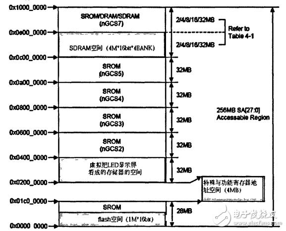
Figure 3--4 System storage space allocation diagram
The theoretical addressing space of the ARM microprocessor is 4GB. It uses a unified addressing method to map various memory types of the system (such as FLASH, SRAM, SDRA~D, peripherals, and special function registers) to the address space. 231. In order to facilitate management, the address space is divided into several small blocks, each of which is called a memory group (MEMORYBANK), and a selection letter of each memory group is usually provided by a hardware circuit.
number. S3C44BOX provides a total of 256MB address space, divided into 8 groups, each group of address space is 32MB, S3CA4BOX [nG-CSo ~ nGCS7l bow l foot g gating these eight sets of address space strobe signal pin field] . The system design storage space allocation diagram is shown in Figure 3.4.
The storage space mapping of the main control board is shown in Table 3.1:
Table 3-l Storage space allocation table
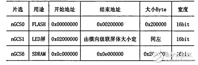
The storage space occupied by the LED display is determined by the horizontal cascading screen number of the LED. For example, for a 512" 256 screen, the horizontal cascading number is 8, and the storage space is: 16*8*16bit total 256 Byte, which can be seen as The address space left by the LED screen is more than enough.
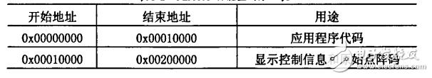
The FLASH address of the main control board ranges from 0x00000000 to 0x00200000, which is 2Mbytes. Its spatial extent is divided into two regional uses as shown in Table 3-2.
Table 3-2 FLASH function space allocation table
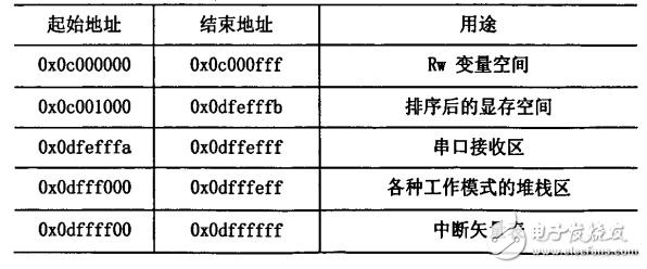
The SDRAM address range of the main control board ranges from 0xoc000000 to 0xodffi. The space allocation and usage are shown in Table 3.3.
Table 3-3 SDRAM function space allocation table
3.3 detailed design of the hardware circuit
3.3.1 Introduction to S3C44BOX
The 32-bit RISC processor S3C44BOX uses the ARM7TDMI core to provide a comprehensive, versatile on-chip peripheral that greatly reduces the configuration of components other than the processor in the system circuit, thereby minimizing system cost. The features of this system are as follows:
(1) 2.5VRISC architecture and ARM7TDMI core processor powerful instruction system, support Thumb code, improve code density; support JTAG on-chip integrated ICE solution.
(2) Support large/small end mode; support 8 memory BANK. 7 of them have a fixed BANK start address and programmable size, 1 has a programmable BANK start address and BANK size;
6 of them support ROM/SRAM access BANK, 2 RohIVS melt RAM access
BANK; all memory BANKs have programmable access operation cycles.
(3) Internally integrated programmable 8KB cache cache, unused cache can be used as 0/4/8kByte SRAM space. A "write-through" strategy that maintains the consistency of the main memory with the cache content.
(4) The on-chip phase-locked loop allows the MCU to operate up to 75MHz.
(5) 30 interrupt sources, using vectorized IRQ interrupt mode to reduce interrupt latency and support
FIQ serves emergency interrupt requests.
(6) 2-channel general-purpose DMA controller, 2-channel interface DMA controller, does not require CPU intervention, supports memory to memory, memory to 10, Io to memory, Io to IO DMA data transfer. And support ontheny mode.
There are many other application resources in S3C44BOX, so I won't go into details here. In this system design, only the 1-channel general-purpose DMA controller and the 1-channel serial UART are used. The internal watchdog timer and the internal 8KSRAM, as well as the PC and PG ports, use a 16-bit bus on the bus selection and make the system work in the small-end mode.
3.3.2 Power Circuit
The main considerations for power circuit design are: power supply type, power-on sequence, digital, analog hybrid power supply processing method, space, input voltage, output voltage, output current, etc., in the main control board of this system, 5V, 3. 3V, 2.5V regulated digital DC power supply. The CPU needs 3.3V and 2.5V respectively to supply power to the on-chip Io port and CPU core, and the LED display interface circuit part needs 5V power supply.
powered by. It should be noted that the CPU core and Io port should be powered according to the kernel before the IO port is powered on, and then the Io port is powered off. However, the time difference between the two should not be too long, otherwise the chip may be destroyed. To simplify the power supply circuit design, a 5V DC switching power supply input is used, and 3.3V and 2.5V DC regulated power supplies are available through the 3.3V and 2.5V linear regulated power supply chips. The circuit is shown in Figure 3.5.
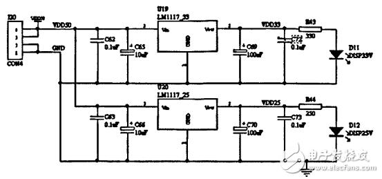
Figure 3-5 Power circuit schematic
3.3.3 crystal reset circuit
Since the serial port of the system uses 9600 baud rate, the system clock used is preferably an integer multiple of 9600. Therefore, the crystal oscillator of 3.6864MHz is selected and the PLL of the S3C44BOX is configured to obtain a system clock of 22.1184MHz, and the S3C44BOX is internally. The PLL circuit has both frequency multiplication and signal amplification. In order to save the cost of the control board, using a passive crystal oscillator, you need to pay attention to:
(1) The selection of the clock source after power-on depends on the logic level state of the OM [3:21 bow 1 pin, as shown in Table 3-4.
(2) The PLLCAP pin of the 3C44BOX needs to be connected to a 680pF compensation capacitor.
(3) The EXTCLK pin of the S3C44BOX needs to be connected to the high level of 3.3v through a 4.7Ω current-limiting resistor, indicating that the clock is not provided using the EXTCLK pin [20-1, as shown in Figure 3-6.
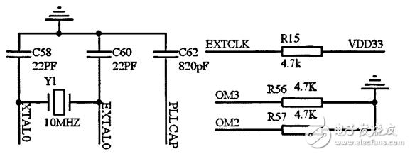
Figure 3-6 Schematic diagram of crystal oscillator circuit
Table 3-4 Clock source selection OM[3:2] configuration table
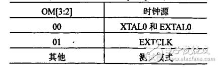
Figure 3.7 shows a simple and practical power-on reset circuit. In the system, the reset circuit mainly completes the power-on reset of the system and the user forces the key reset function while the system is running. The reset circuit consists of a simple Rc circuit, and its reset logic is reliable.
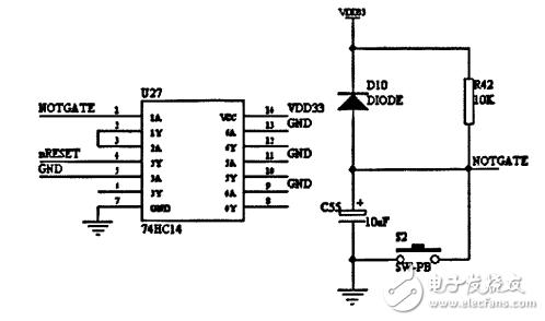
Figure 3-7 Schematic diagram of the reset circuit
The working principle of the reset circuit is as follows: when the system is powered on, the capacitor C55 is charged through the resistor R42. When the voltage across the C55 does not reach the threshold voltage of the high level, the output of the NOTGAATE terminal is low, and the system is in the reset state; When the voltage across C55 reaches a high threshold voltage, the NOTGATE output is high and the system enters normal operation. When the user presses the button S2, the charge at both ends of C55 is discharged through D10 and R42, the output of the NOTGAATE terminal is low, the system enters the reset state, and then the above charging process is repeated, and the system enters the normal working state. NOTGATE uses two-stage non-gate circuit for button debounce and waveform shaping; by adjusting the parameters of R42 and C55, the reset state can be adjusted. It is worth noting that the nRESET of S3C44BOX should last for 4 clocks after power-on. The level, which is 200 ns when the system clock is 22.1184 MHz. However, after power-on, the crystal oscillator of the system often needs 100ms to 200ms to stabilize the pin l. Therefore, the C55 positive electrode should be kept long enough after power-on. The reset time is mainly determined by R and C, C55 positive voltage ore = 3.30 - et / 7), f = RC. Let 0.8V be the upper limit of low level, choose R42 to be 100kQ, C55 is 10uF, and get t*277ms to meet the reset requirement.
3.3.4 FLASH interface circuit
The code of the system and the original dot matrix code received from the host computer and the display control information data are stored in the FLASH chip outside the CPU. When the S3C44BOX is powered on and reset, it immediately fetches from the address of 0x00000000 and starts execution, and locates The memory at address 0x00000000 is called BootROM. Therefore, the startup code of the system should be placed at 0x00000000. In ARM systems, FLASH, which can be quickly read and thus easy to write, is usually used as code and constant memory. The CPU does not require any software configuration on the FLASH interface at power-on, because the default control timing of the internal memory access control register of the S3CA4BOX is slow enough to read the ROM chip data at any speed, but in order to fully exploit the performance of the FLASH chip. The access timing of the corresponding memory should be configured in the initialization. It is worth noting that in order for the CPU to operate FLASH normally, it is necessary to pay attention to two hardware settings: 3cY4, the bus width of the terminal and BANK0. The ARM architecture can store words in two ways (the words here are 32bit or 4Byte), called big endian and little endian. The logic of the input level of the ENDIAN pin of the S3C44BOX determines whether the data type is big endian or small endian [3ll. 0 is the little end, l is the big end. In this system, the small-end mode is used, so the ENDLAN should be connected to the pull-up resistor and grounded. The connection diagram is shown in Figure 3.7.
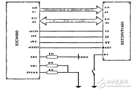
Figure 3-8 Schematic diagram of S3C44BOX and FLASH connection
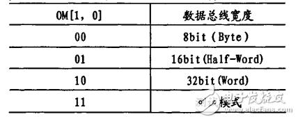
The BOOTROM is located in the BANK0 area of ​​the ARM processor at the address. It may have a variety of data bus widths. This width can be set by hardware, that is, by the logic level on the OM[1, O] pin on the S3C44BOX. Set, as shown in Table 3-5.
Table 3.5 BOOT0 data bus width setting in BANK0
This system uses a SST39VFl601 (1Mxl6bit) as the code and data memory to meet the system requirements, so the system uses a 16bit external bus. Therefore, the OM[1,o]- pin should be set to Ol, and the DWO in the BWSCON register is set to 01 in the initialization routine. This system uses SST39VFl601 in TSOP package. It should be noted that the WP pin of SST39VFl601, when WP is connected to a stable low level, sector O is 1321 that cannot be erased. Only when the WP pin is connected to a stable high level or floating (when the pin is floating, the internal The circuit pulls it high to erase it, so a jumper should be placed at the foot, floated when the program is downloaded, and tied low when the product is running. Since S3C44BOX is addressed by byte, and since SST39VFl601 is 16bit as a storage unit, the address of the processor deviates to the left by one field, and ADDRI is connected with A0 of SST39VFl601, namely: ADDR of S3C44BOX[20:l] Corresponds to A[19:o] of FLASH. Since the mapping of FLASH is in the BANK0 area, the chip selection of SS1"39VFl601 and NGCS0 of S3C44BOX.
3.3.5 SDRAM interface circuit
SDRAM is a volatile memory. After the power is turned off, the data disappears immediately. However, it has the characteristics of fast storage speed, large capacity and low cost. It is widely used in various embedded systems. The system uses 4Mxl6bhx4b£mk, which is 32MByte SDR. The uM chip K4S561632D is used as the R/W segment of the system, the memory, the host communication segment, the interrupt vector table, the memory of the stack data, and the detailed configuration of the storage space. See Section 3.2.2. Due to the characteristics of the SDRAM memory cell circuit, the memory cell can be understood as a capacitor, which always tends to discharge. In order to avoid data loss, it must be periodically charged and refreshed. The S3C4480X chip itself provides a direct interface with DRAM and SDRAM. Because there is no need to program peripheral logic circuits to implement SDRAM refresh timing, only a few memory interface control registers corresponding to the S3C44BOX contents can be properly configured. Figure 3-9 shows the connection between the S3C44BOX and the K4S561632D.
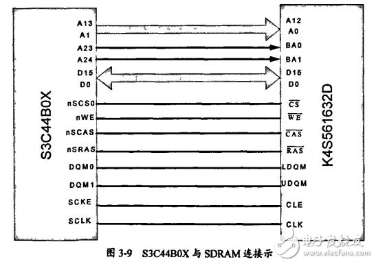
The K4S561632D is a 32MB SDRAM (Synchronous Dynamic Random Access Memory). All input and output signals are the same as the system clock of the CPU's front side bus. Therefore, the S3C4480X provides the synchronous clock pin SCLK, which is connected to the CLK pin of the K4S561632D. .
K4S561632D's storage space organization is: 4M & TImes; 16bit & TImes; 4bank, is a multi-bank structure port '1. As mentioned above, the DRAM memory cell circuit features a capacitor, which needs to be pre-charged before reading the data. The multi-bank structure can be used to read and write to another bank in a bank for pre-charging time. After the fetch, the pre-charged bank can be read immediately, thus eliminating the pre-charging time and greatly improving the access speed of the memory. K4s561632D is divided into 4 banks, which manage 4 banks internally. Control each bank for pre-charging. The BA0 and BAI pins on it are used to select between four banks. Since the capacity of the K4S561632D is 32MB, its BAl and BA2 are connected to the address lines A24 and A23. Due to the need of high-speed digital wiring, in the PCB layout, several important signal line terminals should be connected with 20 ohm impedance matching resistors to ensure that the distortion of high-speed digital signals does not exceed the required range.
The read operation first makes the CKE pin valid, activates K4S561632D, and then a read or write is valid. The activated address is used to select the bank and row for the desired operation (BA0, BAI is used to select bank, A0 way All Used to select rows). After the row address is read and delayed by one to several clocks (latency), the address buses A0 through A8 are used to select the column address at which the operation begins, so that the data is read.
3.3.6 Interface circuit design of main control circuit and LED screen
This display system selects S3C44BOX based on ARM7TDMI core with internal DMA controller as the main controller, so that it works in ARM state. In order to speed up the transmission of data and improve the efficiency of data transmission, the design idea of ​​this system is:
(1) The virtual display of the LED display is regarded as a continuous storage space [3 Xi. C2) Use the DMA controller inside the S3C44BOX to achieve accurate data transmission. During the transmission process, the CPU does not participate, and completes a piece of data transmission during continuous read and write operations.
(3) Using the parallel technology, the data bus of the main control board to the LED screen is 16 bits wide, and data is transmitted to the two display modes of the vertical cascade.
It is possible to treat the LED display as a contiguous storage space as described in Section 2.2.4. It is the basis for completing a data transfer in a continuous read and write operation using the DMA controller. It can be seen from Section 2.2.4 that the decoding circuit and the misalignment cascading on the parallel data transmission display template can accurately align the data latches of each column on each display template and display template, as shown in Figure 2 As shown in Figure 6, the horizontally cascaded display template can be viewed as a contiguous storage unit, so transferring column data to the display driver board is actually a write operation to the memory unit. In this way, the control line of the CPU write memory, the data bus, and the signal appearing on the address bus can be used to transmit the column data to the control signal latched by the first stage column data latch of the display driver board. The decoding signal of the strobe decoder of the first-level column data latch can utilize the address line of the microcontroller. Since there are 16 pairs of latches on one display driver module of the LED display screen, four lower address lines are needed. The first stage column data latches the decoding signal, and the horizontal cascading can cascade up to 8 display driver modules, so three address high address lines are required, but a high address line is reserved for a total of 8 for future expansion. Address line. Column data is transferred by the data bus.
As can be seen from Section 2.2.4, the data bus width on the LED display template of parallel data transmission is 8bit, and the data bus width of the main control board to the LED display is 16bit, so the main control board is on the LED display. A write operation actually transfers data to the same-named column of the same name row of the two display templates of the vertical cascade, which improves the speed and efficiency of data transmission. However, the use of 16-bit wide parallel DMA transmission technology requires the software to first sort the original dot matrix code as required. The sorting algorithm only needs to be run once after receiving the new display content or after power-on, so that the asynchronous display system is acceptable. The algorithm will be discussed in detail in Section 3.4.4. Here we assume that the data in the video memory is sorted as required and can be directly transferred to the DMA.
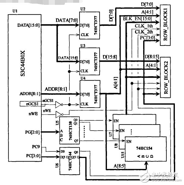
Figure 3-10 Schematic diagram of the main control board and LED screen interface circuit
Therefore, the main control circuit and the LED display interface circuit should be able to achieve the following functions:
(1) Strobe the display module at any position and the first-level column data latch on the module. The dot code to be displayed at the position is accurately latched, and the refresh data can be latched to the second-stage column data latch and output after the data latch of the first-stage column data latch is refreshed.
(2) It can control the strobe drive to drive 16 rows of the same name row for progressive scan display.
(3) Realize the logic level conversion of the main control chip 3.3v to the LED screen 5V 136]. The schematic diagram of the main control board and LED screen interface circuit is shown in Figure 3.10. For a large LED screen, its structure can be divided into vertical cascading and horizontal cascading. This structure is similar to a three-dimensional array. Let's assume a three-dimensional array of LED[i][j]å••, where;
i=0, l'2...,m represents the serial number of the vertical cascade level of the LED screen.
j=O, 1'2..., n represents the serial number of the horizontal cascade of the LED screen.
k=0, l, 2..., 15 represents the serial number of the 16 first-level column data latches on the display module.
Since the system uses the 16-bit parallel bus data transmission method and treats the LED screen as a continuous storage unit, the first-stage column data latch decoder is strobed on the display module using A[4:l] (Fig. 2. The decoding input of 5U2) is the k variable of the three-bit array; the decoder input (Fig. 3-9U7-U15) of the strobe horizontal cascade display module is used as the decoding input of three [8:5]. The j variable of the bit array; because the LED screen requires good flexibility, and because of the technical requirement of the DMA transmission data requiring the dot matrix code storage sequence, the vertical cascade strobe does not satisfy the condition of using the address bus decoding strobe. Therefore, the PG[2:0] of S3C44BOX is used as the decoding input of the vertical cascaded strobe decoder, that is, the i variable of the three-bit array.
Since the state on the address and data bus is constantly changing, when writing to the LED screen
The address and data signals should be latched. The main control board uses U2, U3, and U4 in Figure 3-9 to latch the address on the LED write operation and the state on the data bus. The LED screen is assigned the first address 0x2000000. When writing to it, the nGCS1 and nWE pins of the S3C44BOX will have an active low level of programmable control delay. Let nGCSl be enabled by a non-gate for U2, U3 and U4 to ensure that the signal on the address and data bus is latched only when accessing the LED screen; nWE is passed through a non-gate screen The latch of the first-level column data latch (Figure 2.5U3-U19) enables the control signal to ensure that it is latched only when the refresh data is stable at the input of the column data latch; the PCI0 of the S3C44BOX is made all Latch enable control signal line for the second-stage latch of the screen (Figure 2-5U20.U35); use S3C44BOX
PCI3:0] is the decoding input for the 16-row drive decoder (Fig. 2.5U1). Since only the main control board needs to control the LED screen output during data transmission, no signal feedback is needed, so the interface circuit adopts the cheap 5V power supply HCT circuit chip port 8l [391] scheme, which can satisfy the main control chip 3.3v to The logic level conversion of the LED screen 5v.
When transferring data in DMA, we are more concerned with the write operation of DMA. The timing is shown in Figure 3.1l. At the time of tl, the DMA write operation starts, and the address and refresh data of the corresponding position of the coffee screen appear on the address and data bus; at time t2, the nGCSl pin has an active low level, and the data on the address and data bus is latched to Figure 3-10. In U2-U4, the output is active; at t3, the nwE pin has an active low level. In Figure 3.10, the output data of U2-U4 is latched to the first-stage column data latch of the screen and output. In this way, the main controller completes the refresh of the column data.
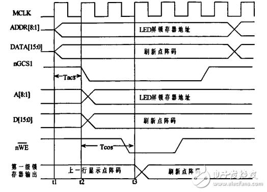
Figure 3.11 DMA write operation timing diagram
3.3.7 Serial Port Circuit Design
In order to weaken the influence of electrical noise on signal transmission, the host computer communicates with the semi-duplex RS485 circuit (4) with complete electrical isolation. The power supply is isolated using a transformer, and the signal and control lines are separated by optocoupler. The circuit is shown in Figure 3-12.
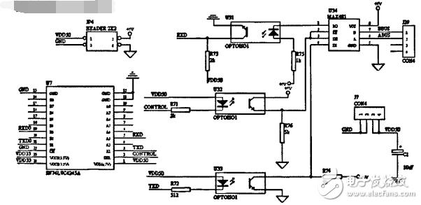
Figure 3-12485 serial port circuit schematic
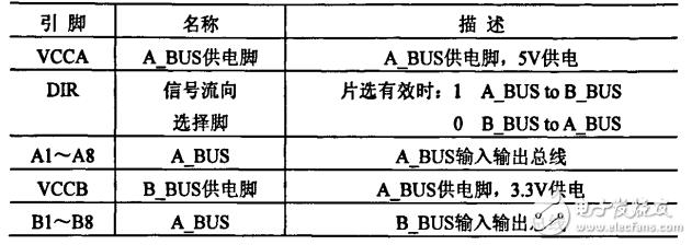
The RS485 replacement chip uses the half-duplex 485 conversion chip MAX481t411. Since the 485 conversion circuit uses 5V power supply, and the main control chip S3C44BOX uses 3.3V power supply, there is a logic level conversion problem. This system uses the SN74LVC4245A which can realize 3.3V to 5v and 5v to 3.3V logic level conversion chip in the serial port circuit. Its pin description is shown in Table 3-6.
Table 3-6 Pin Description of SN74LVCA245A
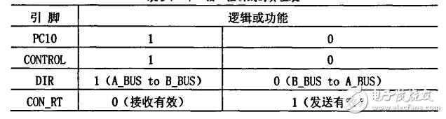
This design uses S3C44BOX's 10-port PCIO for serial port transceiver control line, but there is a problem of logic level conversion. PCI0 firstly obtains 5V logic level signal line CONTROL through 74HCT244 output, which is used as serial port transceiver control line and SN74LVC4245A. The data flows to the control line. The CONTROL control line is isolated by the optocoupler to become the CONRT control line control signal. The truth table is shown in Table 3.7.
Table 3-7 Truth Table of the Serial Interface Control Cable
According to the truth table, the serial port pin RXD0 of the 3.3V logic level of S3C44BOX should be connected to the B bus of SN74LVCA245A; the 5V logic level pins RXD and TXD of 485 serial port should be connected to the A bus of SN74IIVC4245A. .
Ac Gear Motor,Ac Geared Motor,Asynchronous Ac Motor,Asynchronous Ac Gear Motor
NingBo BeiLun HengFeng Electromotor Manufacture Co.,Ltd. , https://www.hengfengmotor.com