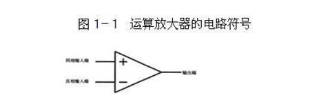
The op amp has two inputs and one output, as shown in Figure 3-1, where the input labeled "+" is the "inverting input" and not the positive terminal), and the other is labeled "one. The “inverting input†of the “number†input can also not be called negative. If the same signal is input from the two input terminals in succession, the output signal with the same voltage but opposite polarity will be obtained at the output: The output signal is in-phase with the in-phase input signal and inverted with the inverting input signal.
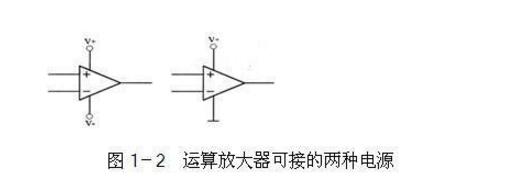
The power supply connected to the operational amplifier can be single-power or dual-power, as shown in Figure 3-1. Operational amplifiers have some very interesting features. Flexible use of these features can lead to many unique uses. In general, these features can be combined into two:
1. The operational amplifier's magnification is infinite.
2. The input resistance of the operational amplifier is infinite and the output resistance is zero.
Now let's briefly look at what conclusions can be drawn from the above two features.
First, the gain of the op amp is infinite, so as long as the input voltage at its input is not zero, the output voltage at the output will be as high as the positive or negative supply. The output voltage should have been infinitely high, but Power supply voltage limit. Specifically, if the input voltage at the non-inverting input is higher than the input voltage at the inverting input, even if it is only a very high point, the output of the operational amplifier will output a voltage that is the same as the positive supply voltage; The input voltage of the phase input is higher than the input voltage of the in-phase input, and the output of the operational amplifier will output a voltage equal to the negative supply voltage (if the operational amplifier uses a single power supply, the output voltage is zero).
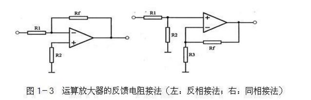
Second, because the amplification factor is infinite, the op amp cannot be used directly as an amplifier. The output signal must be fed back to the inverting input (called negative feedback) to reduce its amplification. As shown in the left picture in Figure 1-3, the function of R1 is to return the output signal to the inverting input of the op amp. Since the voltage at the inverting input is opposite to the output voltage, the circuit's amplification is reduced. , is a negative feedback circuit, resistor Rf is also called negative feedback resistor.
Also, because the input of the op amp is infinite, the input of the op amp has no current input—it only accepts voltage. Similarly, if we imagine an infinite resistance between the non-inverting input and the inverting input of the op amp, the voltage across the resistor will not be able to form a current, and there will be no current. According to Ohm's law, both ends of the resistor There will be no voltage, so we can also think that the two input voltages of the operational amplifier are the same (the voltage in this case is a bit like using a wire to short the two inputs, so we call this phenomenon again "virtual short").
Operational amplifier main parameters1. Common mode input resistance (RINCM) This parameter indicates the ratio of the input common-mode voltage range to the variation of the bias current in this range when the op amp operates in the linear region.
2. DC Common Mode Rejection (CMRDC) This parameter is used to measure the op amp's ability to reject the same DC signal applied to both inputs.
3. AC common mode rejection (CMRAC) The CMRAC is used to measure the op amp's ability to reject the same AC signal applied to both inputs and is a function of the differential open-loop gain divided by the common-mode open-loop gain.
4. Gain Bandwidth Product (GBW) The gain bandwidth product, AOL Æ’, is a constant that defines the region where the open-loop gain vs. frequency characteristic curve rolls off by -20 dB/decade.
5. Input Bias Current (IB) This parameter refers to the average current flowing into the input when the op amp operates in the linear region.
6. Input bias current temperature drift (TCIB) This parameter represents the amount of change in the input bias current when the temperature changes. TCIB is usually expressed in pA/°C.
7. Input offset current (IOS) This parameter refers to the difference between the currents flowing into the two input terminals.
8. Input offset current temperature drift (TCIOS) This parameter represents the amount of change in the input offset current when the temperature changes. TCIOS is usually expressed in pA/°C.
9. Differential Mode Input Resistance (RIN) This parameter represents the ratio of the input voltage variation to the corresponding input current variation. The change in voltage results in a change in current. When measuring at one input, the other input is connected to a fixed common-mode voltage.
10. Output impedance (ZO) This parameter refers to the internal equivalent small signal impedance of the output terminal when the operational amplifier operates in the linear region.
11. Output Voltage Swing (VO) This parameter refers to the peak-to-peak amplitude of the maximum voltage swing that can be achieved without clamping the output signal. VO is generally defined at a specific load resistance and power supply voltage.
12. Power consumption (Pd) represents the static power consumed by the device at a given supply voltage, Pd is usually defined in no-load conditions.
13. Power Supply Rejection Ratio (PSRR) This parameter is used to measure the ability of the op amp to maintain its output when the supply voltage changes. The PSRR is usually expressed as the amount of input offset voltage change caused by a change in the supply voltage.
14. Slew Rate/Slew Rate (SR) This parameter refers to the maximum value of the ratio of the output voltage variation to the time required for this change to occur. SR is usually expressed in units of V/μs, and is sometimes expressed as a positive change and a negative change, respectively.
15. Supply Current (ICC, IDD) This parameter is the quiescent current consumed by the device at the specified supply voltage. These parameters are usually defined under no-load conditions.
16. Unity gain bandwidth (BW) This parameter refers to the maximum operating frequency of the op amp when the open loop gain is greater than one.
17. Input Offset Voltage (VOS) This parameter indicates the voltage difference that needs to be applied to the input when the output voltage is zero.
18. Input offset voltage temperature drift (TCVOS) This parameter refers to the change of the input offset voltage caused by the temperature change and is usually expressed in μV/°C.
19. Input Capacitor (CIN) CIN represents the equivalent capacitance of any input when the op amp operates in the linear region (the other input is grounded).
20. Input Voltage Range (VIN) This parameter refers to the allowable input voltage range when the op amp operates normally (the desired result can be obtained). VIN is usually defined at the specified supply voltage.
21. Input Voltage Noise Density (eN) For an op amp, the input voltage noise can be viewed as a series noise voltage source connected to either input. eN is usually expressed in nV/radical frequency Hz and is defined at the specified frequency.
22. Input Current Noise Density (iN) For op amps, the input current noise can be viewed as two noise current sources, connected to each input and common, usually expressed in pA / root number Hz, defined in the specified frequency.
Operational Amplifier Calculation FormulaOperational Amplifier Magnification Calculation Formula Magnification G=(-)R2/R0, G is independent of R1. To see the details of a tiny object or object, it is necessary to move the object closer to the eye. This will increase the viewing angle and create a larger real image on the retina. However, when the object is too close to the eye, it cannot be seen clearly. To speak in other words, to be able to see clearly, not only should the object have a large enough angle to the eye, but it should also take a suitable distance. Obviously for the eyes, these two requirements are mutually restrictive. If a convex lens is placed in front of the eye, this problem can be solved. The convex lens is the simplest magnifier that is a simple optical instrument that helps the eye to observe tiny objects or details.
Take the convex lens as an example and calculate its magnification. The object PQ is placed between the object focal point of the lens L and the lens and brings it close to the focal point, as shown in Fig. 2-20(a), so that the object forms an enlarged virtual image P'Q' through the lens. If the image focal length of the convex lens is 10 cm, the magnification of the magnifying glass made of this lens is 2.5 times, and it is written as 2.5×. If only from the magnification point of view, the focal length should be shorter, and it seems that this can get arbitrarily large magnification. However, due to the presence of aberrations, the general amplification power is about 3×. If you use a double magnifier (such as an eyepiece), you can reduce the aberration and make the amplification power reach 20×.
What are the commonly used operational amplifier chips?Commonly used low-power op amps: LM324, LM358. Commonly used high impedance op amps: TL082, TL074, CA3140. Commonly used precision op amps: OP07, OP27, ICL7650.
Operational amplifier basic circuitA single-supply op amp requires an external virtual ground. Typically, this voltage is VCC/2. The circuit in Figure 2 can be used to generate a VCC/2 voltage, but it will reduce the system's low-frequency characteristics.
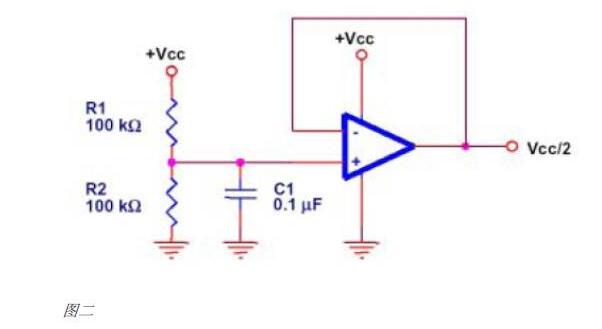
R1 and R2 are equivalent and are selected by the allowable power dissipation and allowable noise. Capacitor C1 is a low-pass filter to reduce the noise from the power supply. Buffered op amps can be ignored in some applications.
High efficient charging speed for Lenovo and IBM laptop, stable current outlet can offer power for the laptop at the same time charge the laptop battery. The best choice for your replacement adapter. We can meet your specific requirement of the products, like label design. The plug type is US/UK/AU/EU.The material of these products is PC+ABS. All condition of our products is 100% brand new.
Our products built with input/output overvoltage protection, input/output overcurrent protection, over temperature protection, over power protection and short circuit protection. You can send more details of this product, so that we can offer best service to you!
Lenovo Adapter,Charger For Lenovo,Power Supply For Lenovo,Adapter For Lenovo Mini
Shenzhen Waweis Technology Co., Ltd. , https://www.waweispowerasdapter.com