Luminous efficiency is a parameter of a light source, which is the ratio of luminous flux to power. Depending on the situation, this power may refer to the radiant flux output by the light source or the energy provided by the light source (which may be electrical energy, chemical energy, etc.). The power in luminous efficiency is usually determined according to the situation, but in many cases it is unclear.
Conversion of luminous efficiencyEach of λ0 and λi is the wavelength of the emission and excitation light. Due to the Stokes shift, there is often a relationship of ηq≥ηp.
Luminous efficiency can also be divided into external efficiency and internal efficiency; the external efficiency only considers the ratio of the output light energy to the light energy or electric energy that is thrown toward the light emitter, and it is the pure conversion efficiency of the absorbed energy into light energy. The input light is lost due to reflection and reabsorption. Therefore, the external efficiency is always less than (or close to) the internal efficiency, and the latter is the true parameter that reflects the energy conversion process.
Fluorescent efficiency of fluorescent lamps
The luminous efficiency reflects the total effect of the internal energy excitation, energy transfer, composite luminescence, and non-radiative recombination process of the luminophore. It is related to the composition of the luminophore, the type and concentration of the luminescent center, the choice of coactivators, and the harmful impurities (annihilation). The central control and the integrity of the light-emitting crystals are even related to the specific process.
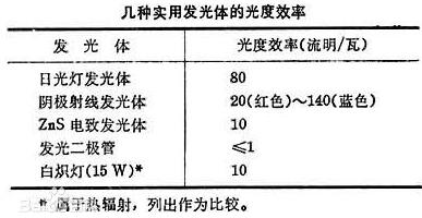
The following table lists the reference values ​​for the photometric efficiencies of several types of practical illuminants:
LED luminous efficiency: Generally known as the external quantum efficiency of the module, which is the product of the internal quantum efficiency of the module and the removal efficiency of the module. The so-called internal quantum efficiency of a component is actually the electro-optical conversion efficiency of the component itself, which is mainly related to the characteristics of the component itself (such as energy bands, defects, and impurities of the component material), the crystal structure and structure of the component, and the like. The removal efficiency of the module refers to the number of photons actually generated outside the module after absorption, refraction, and reflection of the photon generated inside the module. Therefore, the factors regarding the removal efficiency include the absorption of the component material itself, the geometry of the component, the refractive index difference between the component and the package material, and the scattering characteristics of the component structure. The product of the internal quantum efficiency of the component and the removal efficiency of the component is the luminous effect of the entire component, that is, the external quantum efficiency of the component. Early component development focused on improving its internal quantum efficiency. The main method is to improve the quality of the crystal and change the structure of the crystal, so that the electrical energy is not easily converted into thermal energy, which indirectly increases the luminous efficiency of the LED, so that about 70% of theory can be obtained. Internal quantum efficiency, but such internal quantum efficiency is almost close to the theoretical limit. Under such circumstances, it is impossible to increase the total light quantity of the module by increasing the internal quantum efficiency of the module. Therefore, improving the extraction efficiency of the module has become an important research issue. The current method is mainly: changes in the shape of the grain - TIP structure, surface roughening technology.
Led luminous efficiency is generally muchLED efficacy = LED luminous flux (ie, lumens) divided by (normal current drive voltage and current product)
For example: 3528 SMD specification 20mA drive voltage is 3.1V, luminous flux 8.5lm then its light efficiency is: 8.5/(3.1*0.02)=137 lm/W
At present, the general product specification of the high lumen efficiency of a power LED in the market is about 50 lm/W, which does not meet the requirements of household daily lighting. Therefore, there are many problems that need to be solved to make the power-type white LED truly enter the lighting field and realize the daily home lighting. The important one is the luminous efficiency. Although there are many factors that can affect the luminous efficiency of white LEDs, the following factors are worth noting:
1. The width of excitation spectrum of fluorescent powder will also affect the light efficiency of the light.
2. The phosphor powder with a relatively large particle size directly reduces the luminous intensity and has become a fatal injury to many fluorescent powder factories.
3, can directly affect the life of white LED is the anti-aging properties of fluorescent powder, followed by the anti-aging properties of epoxy resin.
4. The reflection efficiency of the LED substrate carrier area or reflector cup lead frame (holder) is also a key factor influencing the luminous intensity.
1, transparent substrate technology InGaAlP
The LED is usually prepared by epitaxially growing a GaP window region of an InGaAlP light emitting region on a GaAs substrate. Compared with InGaAlP, GaAs material has a much smaller bandgap, therefore, when short-wavelength light is emitted from the light emitting region and the window surface into the GaAs substrate, it will be fully absorbed, which is the main reason for the low light output efficiency of the device. . A Bragg reflection region is grown between the substrate and the confinement layer to reflect light perpendicular to the substrate back to the light-emitting region or window, partially improving the light extraction characteristics of the device. A more effective method is to remove the GaAs substrate first and replace it with a fully transparent GaP crystal. Since the substrate absorption region was removed from the chip, the quantum efficiency was increased from 4% to 25-30%. In order to further reduce the absorption of the electrode region, this transparent substrate-type InGaAlP device was fabricated into the shape of a truncated inverted cone, which greatly improved the quantum efficiency.
2, metal film reflection technology
The transparent substrate process first originated from HP, Lumileds and other companies in the United States. The metal film reflection method was mainly performed by Japanese and Taiwanese manufacturers. This process not only avoids the transparent substrate patent, but also more conducive to scale production. The effect can be said to be similar to the transparent substrate method. The process is usually referred to as the MB process. First, the GaAs substrate is removed, and then an Al metal film is vapor-deposited on the surface of the Si substrate at the same time, and then welded together under a certain temperature and pressure. In this way, the light radiated from the light emitting layer to the substrate is reflected by the Al metal film layer onto the chip surface, thereby increasing the luminous efficiency of the device by more than 2.5 times.
3, surface microstructure technology
The surface micro-structure process is another effective technology to improve the light extraction efficiency of the device. The basic point of the technology is to etch a large number of small structures with the size of the light wavelength on the surface of the chip. Each structure is in the form of a truncated tetrahedron, which not only expands The light exit area changes the direction of light refraction at the surface of the chip, resulting in a significant increase in light transmission efficiency. Measurements indicate that the efficiency of light extraction can increase by 30% for devices with a window layer thickness of 20 μm. When the window layer thickness is reduced to 10 μm, the light extraction efficiency will be improved by 60%. For the 585-625nm wavelength LED device, the luminous efficiency can reach 30lm/w after the texture structure is made, and its value is close to that of the transparent substrate device.
4, flip chip technology
A GaN-based LED structure layer is grown on a sapphire substrate by MOCVD technology, and light emitted from the P/N junction light emitting region is emitted through the above P-type region. Due to poor conductivity of P-type GaN, in order to obtain good current spreading, a layer of Ni—Au metal electrode layer needs to be formed on the surface of P region by vapor deposition technology. P zone leads are drawn through the layer of metal film. For good current spreading, the Ni-Au metal electrode layer should not be too thin. For this reason, the luminous efficiency of the device will be greatly affected, usually at the same time taking into account the two factors of current spreading and light extraction efficiency. However, in any case, the presence of the metal film will always deteriorate the light transmission performance. In addition, the presence of wire bonds also affects the light extraction efficiency of the device. The use of a GaN LED flip chip structure can fundamentally eliminate the above problems.
5, chip bonding technology
Optoelectronic devices have certain performance requirements for the required materials, and usually require a large bandwidth difference and a large change in the refractive index of the material. Unfortunately, there is usually no natural material. With homoepitaxial growth techniques, the required bandwidth difference and refractive index difference are generally not formed, and conventional heteroepitaxial techniques, such as epitaxially growing GaAs and InP on a silicon wafer, are not only more costly but also combine interface bits. The wrong density is also very high and it is difficult to form high quality optoelectronic integrated devices. Because of the low temperature bonding technology, the problem of thermal mismatch between different materials can be greatly reduced, and stress and dislocation can be reduced, so that a high quality device can be formed. With the gradual understanding of the bonding mechanism and the maturation of the bonding process technology, it has become possible to bond the chips of many different materials to one another, thereby possibly forming materials and devices for special applications. A new structure can be formed by forming a silicide layer on a silicon wafer and then bonding. Due to the high conductivity of the silicide, it can replace the buried layer in bipolar devices, reducing the RC constant.
6, laser stripping technology (LLO)
Laser lift-off technology (LLO) uses laser energy to decompose the GaN buffer layer at the GaN/sapphire interface to separate the LED epitaxial wafer from the sapphire substrate. The technical advantage is that the epitaxial wafer is transferred to a high thermal conductivity heat sink, which can improve the current spreading in large-size chips. The n-plane is the light-emitting surface: the light-emitting area is increased and the electrodes are light-blocked, which facilitates the preparation of the microstructure and reduces the etching, polishing, and dicing. What's more important is that the sapphire substrate can be reused.
ZGAR GenkiIppai Pods 5.0
ZGAR electronic cigarette uses high-tech R&D, food grade disposable pod device and high-quality raw material. All package designs are Original IP. Our designer team is from Hong Kong. We have very high requirements for product quality, flavors taste and packaging design. The E-liquid is imported, materials are food grade, and assembly plant is medical-grade dust-free workshops.
From production to packaging, the whole system of tracking, efficient and orderly process, achieving daily efficient output. WEIKA pays attention to the details of each process control. The first class dust-free production workshop has passed the GMP food and drug production standard certification, ensuring quality and safety. We choose the products with a traceability system, which can not only effectively track and trace all kinds of data, but also ensure good product quality.
We offer best price, high quality Pods, Pods Touch Screen, Empty Pod System, Pod Vape, Disposable Pod device, E-cigar, Vape Pods to all over the world.
Much Better Vaping Experience!


ZGAR GenkiIppai 5.0 Pods,ZGAR GenkiIppai Pods 5.0,ZGAR GenkiIppai Pods 5.0 Pod System Vape,ZGAR GenkiIppai Pods 5.0 Disposable Pod Vape Systems, Japanese culture style
Zgar International (M) SDN BHD , https://www.szvape-pods.com