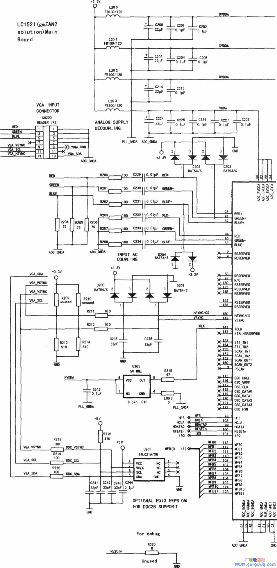
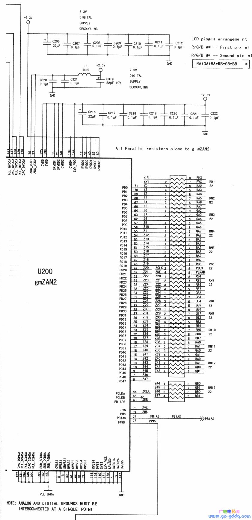
gmZAN2 is a kind of ultra-large-scale image digital processing circuit, mainly used in Konka LC-1521T liquid crystal color TV. As shown in the figure, the functions of its pins are mainly:
(1)(8)(18)(30)(41)(49)(61)(72)(114)(126)(140)(151)(158)(5)(59)(147)foot, Ground.
2 feet (RESERVED), reserved terminal U, unused.
3 feet (PSCAN), not used.
4 feet (RESERVED), reserved port, unused.
6 feet (PD47), display port 47, unused.
7 feet (PD46), display port 46, unused.
9 pin (PD45), display port 45, for RB1 output, sent to RN12.
Pin 10 (PD44), display port 44, for RBO output, is sent to RN12.
(11) (21) (58) (125) (139) (149) feet, +2, 5V power supply.
(12) (33) (40) (65) (60) (108) feet, +3.3V power supply.
(13) Foot (PD43), display port 43, for BA1 output, sent to RN12.
(14) Foot (PD42), display port 42, for BAO output, and sent to RN12.
(15) Foot (PD41), display port 41, output with rGAI, and sent to RN11.
(16) Pin (PD40), display port 40, for GAO output, and sent to RN11.
(17) Pin (PD39), display port 39, for RA1 output, and sent to RN11.
(19) Foot (PD38), display port 38, for RAO output, sent to RN11.
(20) Foot (PD37), display port 37, for BB7 output, sent to RN10.
(22) Foot (PD36), display port 36, for BB6 output, and sent to RN10.
(23) Foot (PD35), display port 35, for BB5 output, and sent to RN10.
(24) Pin (PD34), display port 34, for BB4 output, sent to RN10.
(25) Pin (PD33), display port 33, for BB3 output, and sent to RN9.
(26) Pin (PD32), display port 32, for BB2 output, sent to RN9.

gmZAN2 image digital processing control circuit (a)
(27) Foot (PD31), display port 31, for GB7 output, sent to RN9.
(28) Pin (PD30), display port 30, for GB6 output, sent to RN9.
(29) Pin (PD29), display port 29, for GB5 output, sent to RN8.
(31) Pin (PD28), display port 28, for GB4 output, sent to RN8.
(32) Pin (PD27), display port 27, for GB3 output, sent to RN8.
(24) Foot (PD26), display port 26, for GB2 output, sent to RN7.
(35) Pin (PD25), display port 25, for RB7 output, and sent to RN7.
(36) Pin (PD24), display port 24, for RB6 output, and sent to RN7.
(37) Pin (PD23), display port 23, for RB5 output, and sent to RN7.
(38) Pin (PD22), display port 22, for RB4 output, and sent to RN7.
(39) Foot (PD21), display port 21 for outputting the PENAB control signal.
(42) Pin (PD20), display port 20, for outputting the PCLK clock signal.
(43) Foot (PDISPE) for ZDE control.
(44) Pin (PCLKA) for ZCLK control.
(45) Foot (PCLKB), unused.
(46) Pin (PD19), display port 19, for RB3 output, and sent to RN6.
(47) Pin (PD18), display port 18, for RB2 output, and sent to RN6.
(48) Pin (PD17), display port 17, for BA7 output, sent to RN5.
(50) Foot (PD16), display port 16, for BA6 output, and sent to RN5.

gmZAN2 image digital processing control circuit (b)
(54) Pin (PD12), display port 12, for BA2 output, sent to RN4.
(55) Pin (PD11), display port 11, for GA7 output, and sent to RN4.
(56) Pin (PD10), display port 10, for GA6 output, sent to RN4.
(57) Pin (PD9), display port 9, for GA5 output, sent to RN3.
(62) Pin (PD8), display port 8, for GA4 output, sent to RN3.
(63) Pin (PD7), display port 7, for GA3 output, sent to RN3.
(64) Pin (PD6), display port 6, for GA2 output, sent to RN3.
(66) Pin (PD5), display port 5, for RA7 output, sent to RN2.
(67) Pin (PD4), display port 4, output with rRA6, and sent to RN2.
(68) Pin (PD3), display port 3, for RA5 output, sent to RN2.
(69) Pin (PD2), display port 2, for RA4 output, sent to RN2. Its output signal is sent to CN202 as shown below.

CN202/CN203 LCD pin circuit
(70) Pin (PD1), display port 1, for RA3 output, fed to RNI.
(71) Pin (PDO), display port 0, for RA2 output, sent to RN1.
(73) Foot (PVS) for ZVS input (field pulse input).
(74) Foot (PHS) for ZHS input (line pulse input).
(75) Foot (PBIAS) for PBIAS control.
(76) Foot (PPWR) for PPWR (standby) control.
(77) (79) foot, +2.5V power supply.
(78) (80) foot, analog/digital circuit is grounded.
(81) (82) (85) (89) (93) Foot, ground.
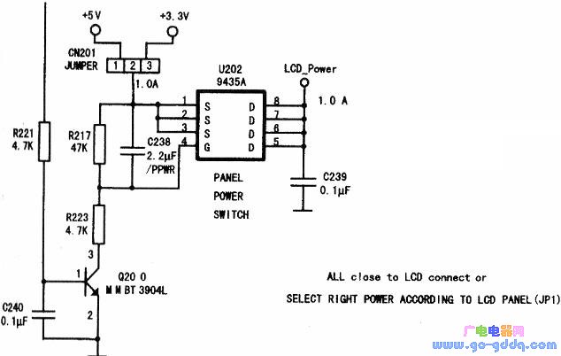
(84) (88) (92) (96) pin, +3.3V power supply. Controlled by U202, as shown in Figure 1-20.
(83) Foot (RESERVED), not used.
(86) Foot (BLUE-), blue base color negative input.
(90) Foot (GREEN-), green base color negative input.
(91) Foot (GREEN+), green color positive phase input.
(94) Foot (RED-), red base color negative input.

U202/(9135A) power control circuit
(95) Foot (RED+), red base color positive input.
(97) Foot (N/C), not used.
(98) Foot (HFS), line pulse input.
(99) (HDATA), data bus input/output.
(100) (RESETn), reset.
(101) Foot (IRQ), remote control signal input.
(102) Pin (MFB9) for HDATA3 data bus input/output.
(103) Pin (HCLK), clock signal input.
(104) pin (MFB8) for HDATA2 data bus input/output.
(105) pin (MFB7) for HDATA1 data bus input/output.
(106) Foot (MFB6), external 10kΩ resistor to ground.
(107) Foot (MFB5), external 10kΩ resistor to ground.
(109) Foot (MFB4) for RIGHT control.
(110) foot (MFB3) for SELECT control.
(111) foot (MFB2) for PWR-SW control.
(112) foot (MFBl) for MENU menu selection
(113) Foot (MFBO) for LEFT control.
(115) Foot (OSD_HREF), not used.
(116) Foot (OSD_VREF), not used.
(117) Foot (OSD_CLK), unused.
(118) Foot (OSD_DATAO), not used.
(119) Foot (OSD_DATAl), unused.
(120) Foot (OSD_DATA2), not used.
(121) Foot (OSD_DATA3), not used.
(122) Foot (OSD_FSW), not used.
(123) foot (MFB11) for LEDORANGE control.
(124) Foot (MFB10) for LED-GRN-EN control.
(127) (131) (134) (138) (144) (133) (132) (146) Foot, ground.
(130) Foot (RESERVED), not used.
(135) Foot (RESERVED), not used.
(141) Foot (TCLK), 50MHz clock signal input.
(142) Foot (XTAL/RESERVED), not used.
(145) Foot (RESERVED), not used.
(148) Foot (VSYNC), field sync pulse input.
(150) pin (HSYNC/CS), line sync pulse input / chip select pulse input.
(152) Foot (RESERVED), not used.
(153) Foot (STl-TMl), not used.
(154) Foot (STl-TM2), unused.
(155) Foot (SCAN.INl), not used.
(157) Foot (SCAN-IN2), not used.
(159) Foot (SCAN-OUTl), not used.
(160) Foot (SCAN-OUT2), not used.
ShenZhen Antenk Electronics Co,Ltd , https://www.atkconnectors.com